 Grounding pattern making Grounding pattern making
In case of making of a PCB, there is technique which makes a wide grounding pattern except the signal and power pattern. This technique is used for the circuit for the high frequency or when preventing an influence by the noise from outside, and so on. When making a printed board by the handwork, there is an effect which can rarely make the quantity of the copper to dissolve, too.
A polygon function is used to draw such a grounding pattern.
 Schematic Schematic
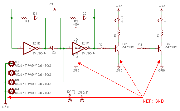
This time, the circuit to use as the example is A-stable multivibrator ( IC type ).
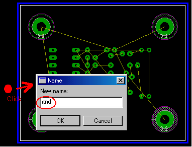
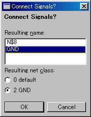
When drawing a schematic, it makes the name of the grounding wire(NET) a GND. You can use a name except the GND. In my case, I am using a grounding symbol and because the symbol name is GND, the name of the wiring becomes GND automatically. This name is used for the name of the polygon. So, it's better to confirm the name of the grounding wire by the Info command after drawing a schematic.
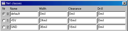
I set the following to Net Class.
Board
After drawing a schematic, create a board using the board button.
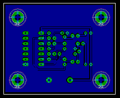
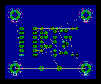
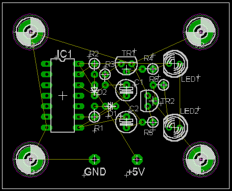 This board is in the condition which the arrangement of the part was ended and the position of the name was adjusted.
A pattern isn't drawn yet.
This board is in the condition which the arrangement of the part was ended and the position of the name was adjusted.
A pattern isn't drawn yet.

When pushing the polygon button, following icon bar is displayed. The property of the polygon is set with these icons.

| Layer |
This is the layer specification of the polygon to draw.
1 is the component side (auburn) and 16 is the wiring side (dark blue). |
| Bend Angle |
This is the bend angle specification when making a polygon.
From left
 0 : Starting point - horizontal - vertical - end 0 : Starting point - horizontal - vertical - end
1 : Starting point - horizontal - 45° - end
2 : Starting point - end (straight connection)
3 : Starting point - 45° - horizontal - end
4 : Starting point - vertical - horizontal - end |
| Width | This is the specifying of the precision to draw a polygon. Usually, the width which is the same as the signal pattern is good. The setting unit is an inch. |
| Pour | This is a pouring pattern specification. Left is Solid. Right is Hatch. |
| Terminal | This is a shape specification for the terminal which is connected with the polygon. Left(off) is combining. Right(on) is showing. |
| Orphan | This is the specification of the blank area of the polygon. Left(off) is no making up with polygon. Right(on) is making up with polygon. |
| Isolate | This is the interval specification between the signal pattern and the polygon. When this set value is smaller than the value specifying by DRC(Design Rule Check) or Net Class, either of DRC or Net Class a big value is used. The default is 0. The setting unit is an inch. |
| Spacing | When "Hatch" is selected by the item of pour, this is the interval specifying of the hatch. The setting unit is an inch. |
| Rank | This is the priority specifying of a polygon. It is effective when more than one polygon is piled up. When the figure is small, the priority is high. "1" is a top priority. |
At the linked item, concrete example is shown.
It is necessary that the property of the polygon is set before drawing a polygon.
Specifying of the polygon area
After polygon setting, create a polygon.
In the example this time, I set a polygon as follows.
| Layer : | 16 Bottom |
| Bend Angle : | 0 |
| Width : | 0.016 |
|
| Pour : | Solid |
| Terminal : | on |
| Orphan : | on |
|
| Isolate : | 0 |
| Spacing : | 0.05 |
| Rank : | 1 |
|
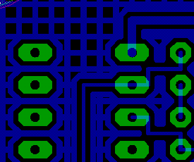
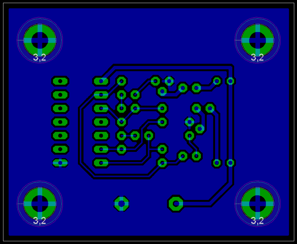
I set "21 tPlace" of Display off to make it easy to see a pattern.
By this, the part shape, the name and so on are made a non-display.
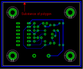
Draw a polygon for the grounding in the periphery of the printed board area.
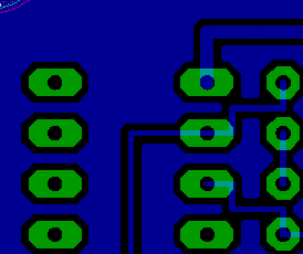
Creating of signal patterns
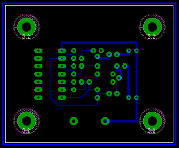
I create signal patterns by the Auto icon.
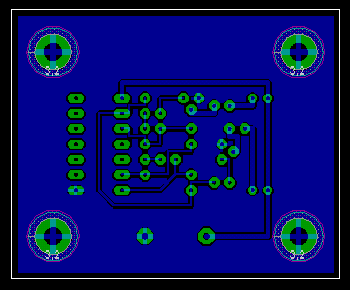 |
This time, I set "1 Top" of Preferred Directions in "N/A" and drawing a pattern only at Bottom(wiring side).
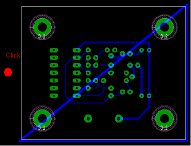
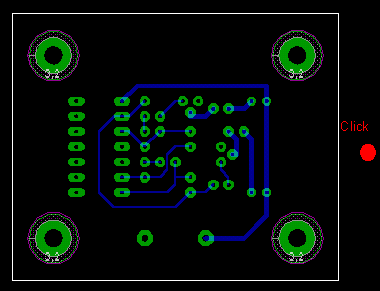
A magnification is shown when you click a figure on the left. |
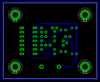
Change polygon display mode
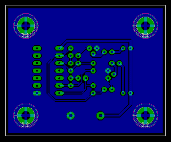
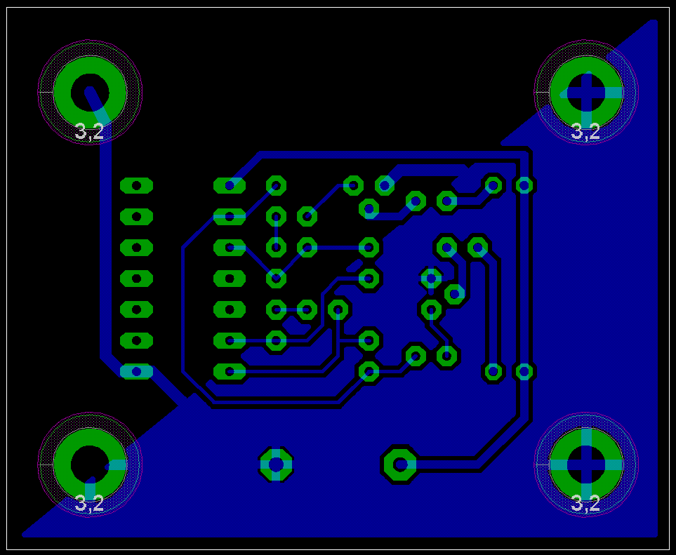
The display mode of the polygon has two types. It is an outline mode and a real mode.
As for the outline mode, only the frame of the polygon is shown at the periphery of the board and the polygon isn't drawn in the board. This mode is convenient when changing a pattern and so on.
As for the real mode, a polygon is drawn in the board. This mode is convenient to confirm the condition of the polygon.
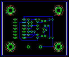
Outline mode |
Real mode |
 Changing into the real mode from the outline mode Changing into the real mode from the outline mode
It switches over to the real mode when pushing the Ratsnest button at the time of the outline mode.
Changing into the outline mode from the real mode
Push the Ripup button at the time of the real mode. Next, it switches over to the outline mode when clicking the outside of the board. Because Ripup has the function to return a pattern to the origin, it is necessary to operate 2 steps.
After changing a mode, the color of the displaying sometimes becomes thin yellow. In this case, it becomes beautiful with the restatement by  . .
Only the data of the outline mode is recorded to the file of EAGLE. The displaying of a real mode is shown with the CAM processor from the data of the outlines. A CAM processor is started up by Ratsnest and real mode displaying is done. An outline mode is shown when restarting a project.
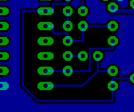
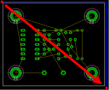
Correction of the signal pattern
When correcting a signal pattern, it makes an outline mode. This is because the pattern is easy to see. It is possible to correct on the real mode, too.
 |
The polygon is drawn around the board and can do the confirmation of the signal pattern easily.
As for the detailed the pattern correction technique, refer to "Correction of the pattern". |
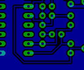
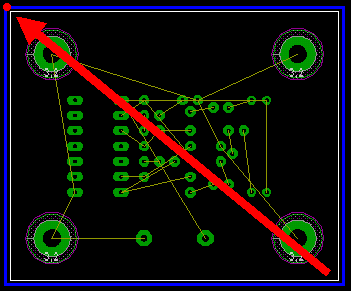
 |
I changed the corner of some patterns. |
 |
When making display a polygon again, it uses the Ratsnest button.
A polygon is drawn according to the corrected pattern.
It is completion.
A magnification is shown when you click a figure on the left. |
Deleting of a polygon
When changing the property of the polygon or stopping the use of the polygon, the polygon must be deleted. There seems to be a polygon in the board when drawing a polygon. However, the polygon in the board is not substance. The polygon is in the periphery of the board. Delete is used for the deleting of a polygon. is used for the deleting of a polygon.
 |
The line of the polygon appears around the board when making an outline mode. This is substance.
To delete the polygon, this substance must be deleted. |
 |
After pushing Delete icon, click the outside of the substance of the polygon.
By this, two lines of the polygon are deleted. Because the lines which form a polygon area are to be always connected.
When clicking Auto in this condition, a polygon in the area of the triangle is drawn.
To find out in this is that it is possible to draw a polygon only in the specific area of the board. |
 |
A polygon is deleted when clicking the opposite side.
Because three lines are necessary even if it is minimum to form a polygon area, when one line of the triangle is deleted, the polygon area becomes extinct. |
Width
The detailed drawing of a polygon can be specified by Width. However, the polygon which was drawn in detail than the precision which makes an actual printed board doesn't have a meaning. At the manual of EAGLE, it is referred to with "Typically you should keep the polygon width in the same range as your other wires".
When drawing a polygon with the hatch, width becomes the width of the line of the hatch.
Width : 0.016 inches |
Width : 0 inches |
Pour
The pattern of the polygon can be specified. Generally, it specifies Solid but in case of which wants to make weight light(?), and so on, it specifies Hatch.
In case of Solid. |
In case of Hatch.
Hatch interval : 0.05mil |
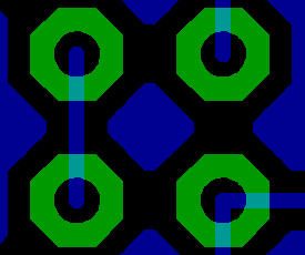
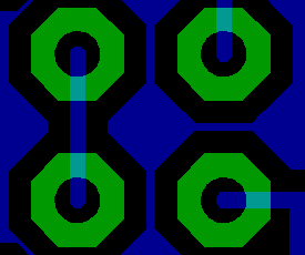
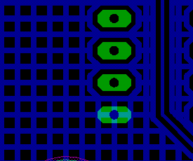
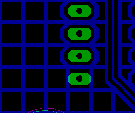
Terminal
There are two kinds of ways of connecting between the earth terminal and the ground pattern. First, the method of making a terminal and a ground pattern incorporated and not leaving a shape. The 2nd, the method of connecting the shape of the terminal by leaving it. In case of the method of leaving the shape of the terminal, a terminal and a ground pattern are connected at four. I think that it is better to leave the shape of the terminal to solder beautifully.
When not leaving the shape of the terminal. (off) |
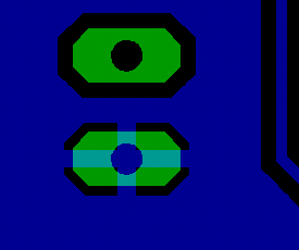
When leaving the shape of the terminal. (on) |
Orphan
When surrounding a signal pattern by the ground pattern polygon, the area where it isn't possible to draw a ground pattern polygon sometimes exists. This is the specifying whether creates or doesn't create a polygon to those areas. The polygon which was created in these areas is connected with nowhere. In case of the high frequency circuit, these patterns sometimes influence circuit operation. In the such case, it should not create the polygon to fill an area.
When not creating polygons, (off) |
When creating polygons. (on) |
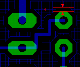
Isolate
The default value of Isolate is 0. In this case, the interval between the signal pattern and the polygon is drawn with the big value either of DRC or NetClass. In case of the Isolate value exceeds the value which is specified by DRC or Net Class, the set value is effective.
The minimum clearance in DRC is 8mil but 16 mil is set to the clearance of GND in Net Class.
For easy to find out, a polygon is drawn with the hatch in the 0.01 inches(10mil) interval. |
Isolate : 0 inches
0.016 inches are set in Net Class |
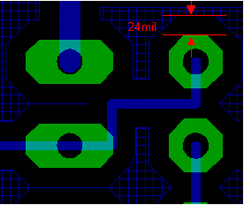
Isolate : 0.024 inches (About0.6mm) |
Spacing
The hatch interval when drawing a polygon with the hatch is specified by this. When Spacing is narrower than Width, because the line of the hatch overlaps, it becomes the same as Solid.
Spacing : 0.05 inches |
Spacing : 0.1 inches |
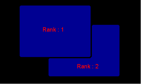
Rank
The priority rises when the specifying value is small. When the polygon overlaps, a polygon with the higher priority is drawn.
|


