CCP feature of PIC16F873
|
The PIC16F873 has a special feature as CCP.
CCP is the initial of Capture/Compare/PWM(Pulse Width Modulation). PIC16F873 has two CCP modules.
The timer resource of the capture and compare is timer1 and the timer resource of PWM is timer2. CCP1 and CCP2 can be worked at the same time. However, because they are using the same timer resources, the interaction occurs. Interaction is shown below.
CCP2 register is comprised of two 8 bits registers : CCPR2L for low byte and CCPR2H for high byte. The CCP2CON register controls the operation of CCP2. The special event trigger is generated by compare match and will reset Timer1 and start an A/D conversion if the A/D modules is enabled. Following, I will explain the operation of CCP1. CCP2 operates the same as CCP1, except where noted. In Capture mode, CCPR1H : CCPR1L captures the 16 bits value of the TMR1 register when an event occurs on pin RC2/CCP1. In Capture mode, the RC2/CCP1 pin should be configured as an input by setting the TRISC register. If the RC2/CCP1 pin is configured as an output, a write to the port can cause a capture condition. 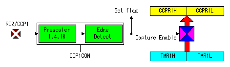
Timer1 must be running in timer mode or synchronized counter mode for the CCP module to use capture feature. In asynchronous counter mode, the capture operation may not work. When the capture mode is changed, a false capture interrupt may be generated, You should keep bit CCP1IE of PIE register clear to avoid false interrupts and should clear the flag bit CCP1IF of PIR1 register following any such change in operating mode. In Compare mode, the 16 bits CCPR1 register value is constantly compared against the TMR1 register pair value. 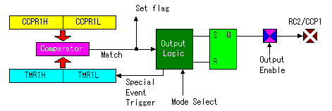 When a match occurs, the following actions will be done by the definition of CCP1M3:CCP1M0 of CCP1CON register.
Timer1 must be running in timer mode or synchronized counter mode for the CCP module to use compare feature. In asynchronous counter mode, the compare operation may not work. In PWM(Pulse Width Modulation) mode, the CCPx pin produces up to a 10 bits resolution PWM output. 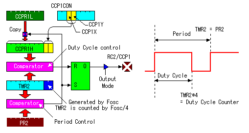
The PWM period is specified by the value of the PR2 register, the clock oscillation period and the prescaler value of Timer2. The PWM duty cycle( the output stays high ) is specified by the value of CCPR1L register, the clock oscillation period and the prescaler value of Timer2. The CCPR1L contains the eight MSbs and CCP1X:CCP1Y contains the two LSbs. The shortest duty cycle is the period time of the oscillator. In case of 10MHz oscillator, it is 0.1 microseconds. The maximum PWM resolution of the duty cycle is 1024. If the PWM duty cycle value is longer than the PWM period, the CCP1 pin will not be cleared. Also, if the value of PWM duty cycle register( CCPR1L+CCP1X+CCP1Y ) is set to zero, the CCP1 pin will not be set. The PWM period is the time which matches TRM2 and PR2. It can be calculated using the following formula. PWM period = (PR2+1) x 4 x Tosc x TMR2 prescale value
The duty cycle is the time which the output stays high. It can be calculated using the following formula. PWM duty cycle = ( CCPR1L+CCP1X+CCP1Y(10bits) ) x Tosc x TMR2 prescale value
This value is the value that 1/1024 is shorter than PWM period compared with example 1. You find that the PWM duty cycle can be controlled in the precision of 1024 pieces of division to the PWM period.
You find that the minimum value of the PWM duty cycle is an oscillator period. CCPR1L+CCP1X+CCP1Y can be written to at any time, but the duty cycle value is not latched into CCPR1H until after a match between PR2 and TMR2 occurs. In PWM mode, CCPR1H is a read-only register. The following steps should be taken when configuring the CCP module for PWM operation. 1. Set the PWM period by writing to the PR2 register. 2. Set the PWM duty cycle by writing to the CCPR1L register and CCP1X and CCP1Y bits of CCP1CON register. 3. Make the CCP1 pin an output by clearing the TRISC. 4. Set the TMR2 prescale value and enable Timer2 by writing to T2CON register. 5. Configure the CCP1 module for PWM operation. |