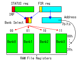
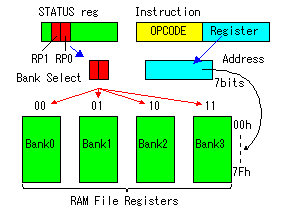
STATUS ( Status register ) 03h,83h,103h,183h STATUS ( Status register ) 03h,83h,103h,183h
By this register, the bank specification of the RAM file register, the time-out condition of the watchdog timer, the power down condition, the flag of the calculation result and so on, are managed.
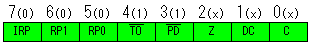
The value in the parenthesis is in the condition immediately after the turning on.
FSR ( Indirect address register ) 05h,85h,105h,185h
| This is the register to specify the address of the register with indirect address mode. |
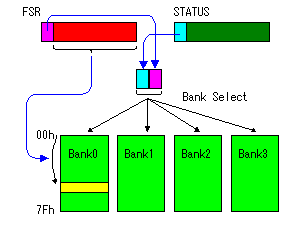 |
The highest bit of FSR is used for the lower bit of the bank specification and a register address in the bank is specified by 7 bits of the remainder. The upper bit of the bank specification is specified by IRP of STATUS register. As for this, refer to the item of the STATUS register.
As for the reading or writing of the register which was specified by FSR, refer to the item of the INDF register. |
PORTn (Port register)/TRISn (Port mode set register) 05h,06h,07h,106h/85h,86h,87h,186h
| PORTn register is the register which does data in or data out from/to the input/output port. TRISn register is a register to set a mode(in/out) of the port. In PIC16F873, the "n" is from A to C and there are not D and E. The A port is 6 ports (using lower 6 bits) and B and C are 8 ports. |
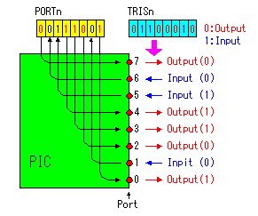 |
The input/output specification of each port is done with the TRISn register. In case of output, it is "0" and in case of input, it is "1".
The data which was set to the PORTn register is output at once. The input data always appears at the PORTn register. The input data can be taken in if reading PORTn register. |
|