Making of the mask pattern by Visio
 |
|
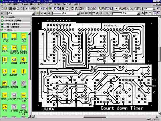
The figure above is the screen which is making the mask pattern using "Visio Technical (R) 4.1J for Microsoft Windows - The professional technical drawing software - Japanese edition". Because it is raising the compression percentage of the picture to make the file size small, it is a little blurred. Visio is not the CAD(Computer Aided Desing : The tool which makes the electric circuit, the pattern drawing and so on automatically). This is the tool to draw a picture. As for Visio, refer to the following site. http://www.microsoft.com/office/visio/ The yellow symbol which is stored in the left frame of the screen is called the stencil. It is the symbol of the diagram. They are the symbol of the resistor, the symbol of the capacitor, the symbol of the grounding and so on. When picturing the electric circuit, you can picture the symbol by drag and drop only. You can expand or reduce the symbol which was arranged in the drawing. When picturing the mask pattern figure, it is possible to picture if there are a square, circularity, a line. I write the point of my style below. Of course, it may picture in the other way. Utilize if becoming your reference. 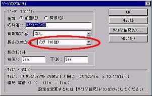 In the pin interval of the DIP-type IC, it is made the standard in the inch. Because it is, it is necessary to specify by the inch in the interval of the land (making the circular pattern on the printed board) to do the soldering, too. The Visio has the function to make the object adhere to the grid. When specifying the length by the inch unit, in the grid interval, it is made the inch. The red circle in the figure shows the specification of the inch unit. (Japanese edition) 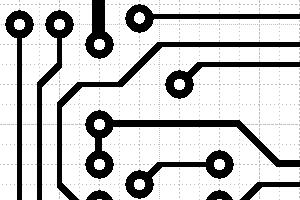 The line of the 3 pixels is used for the signal line with the flowing weak electric current. The line of the 3 pixels has melted when the printed board etching is long. You must confirm the result condition of the etching briskly. The thick line is used for the power supply line. 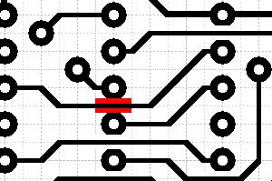 I am using the circle with the 0.069-inch diameter for the land. The white circle with the central part has the 0.032-inch diameter. The other size was good but I did to this size. Because it is the 0.1 inches in the pin interval of the DIP-type IC, the crack of the land is 0.1-0.069 = 0.031 inches. The interval of the land and the line is narrow when passing the line of the 3 pixels through this crack. Therefore, I put on the rectangular mask on the land. The lands are shaved a little and the interval with the line opens. In the figure, I did to the red to make it easy to see the mask. The actual mask is made white so as not to be able to be seen. |