Circuit explanation
of CPLD Programmer
|
The main part of circuit is based on the information which the Xilinx Inc. makes open on the following site for the person who want to build own download cable. JTAG Parallel Download Cable Schematic 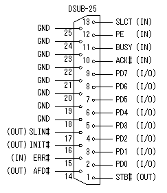 The CPLD programmer is connected with the parallel port of the personal computer. A printer is generally connected with the parallel port. The figure on the left shows the signal of each pin of the parallel port. A pin numbering is written by the small character at the connector. Because the assignment position with number becomes opposite on the side of the male connector and the side of the female connector, make not make a mistake. The 1st pin is connected with the 1st pin of the opposing connector. At the equipment this time, each pin is used as follows.
In the table above, the IN and OUT are the direction of the signal which was seen from the side of the personal computer. It becomes contrary to the seeing from the side of the equipment.
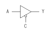
A bus buffer is put in the signal conductor of JTAG(TMS, TCK, TDI and TDO). 3 State buffer is used for buffer circuit. By this, the writing circuit to the CPLD device doesn't influence the parallel port of the personal computer. The buffer circuit works only when transferring data with the CPLD device. When not transferring data, the output of the buffer becomes high impedance and becomes the condition which was separated from the circuit. When the transfer of the data is done, the buffer becomes low impedance to the CPLD device and makes the writing of data possible. When the C terminal is H level, output terminal (Y) becomes high impedance. In this condition, it becomes the same when a bus buffer isn't connected. When the C terminal becomes an L level, the condition of input terminal (A) comes out to output terminal (Y). Because there is a high impedance condition in addition to H level and L level, this buffer is called a 3 State buffer. In the table, Z shows a high impedance condition. 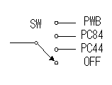 A device is switched by the rotary switch. Either one device can be controlled. Because it uses only any one generally, it is to be OK even if it doesn't switch. In the case, it is necessary to be careful when using. In case of the PWB mode, the power supply to the CPLD device uses the outside power. It is possible to use the power of this equipment only in about 100 mA.
Because the red LED is during the blink while forwarding data, don't dissolve to switch off the power, to pull out a cable and to remove a device. To make an influence over the TDI-signal little, the value of the resistor to be putting in the LED in series is big comparatively. 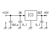 This power circuit makes the stable voltage(+5V) which the bus buffer and the CPLD device needs. 3 terminal regulator is used to get +5V output from +12V power in. |