Block diagram of XC9500 series
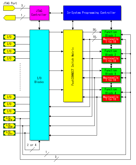 You can jump to the page of the explanation when you click the part where the pointer become the hand. If you want to know more detailed specification, refer to the following PFD file. XC9500 5V ISP CPLD Family 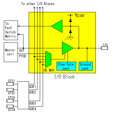 An I/O block is composed of input buffer, output buffer, multiplexer for the output control and grounding control and so on. Multiplexer for the output control(OE MUX) controls an output enable or stop. It is controlled by the signal from the macrocell or the signal of the GTS(Global Three-State control) pin. It can always make output '1' or '0', too. There are four GTS in XC95216 and XC95288 and in case of the other device, they are two. A slew rate control is the one to make the rising and the falling of the output pulse smooth. It is used when suppressing the occurrence of the noise. A grounding control is used when making input/output pin (I/O) an earth terminal. In case of the circuit where much noise occurs, it isn't sometimes possible to do noise reducing by the standard earth terminal. At the actual circuit, a pull-up resistor is more connected with the input/output pin. This circuit makes an input/output pin '1' condition compulsorily during programming of CPLD to make an influence by the condition of the I/O pin little. This circuit is detached in usual operation. Each input/output pin can handle a 24-mA current. 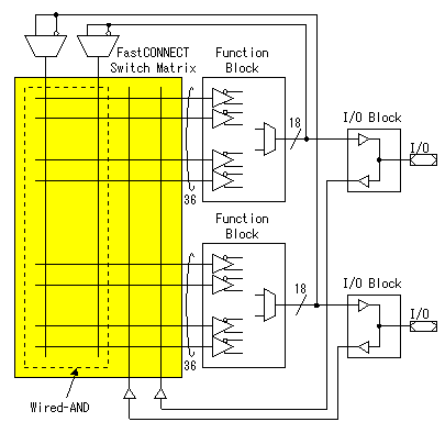 FastCONNECT Switch Matrix controls the input signals to the Function Block. All the signals from the input-output port and the signals of the Function Block are connected with FastCONNECT Switch Matrix. The signals which are specified by the program out of these signals are applied to the Function Block. The output signals from the Function Block are applied to the Function Block through the wired AND buffer. This provides additional logic capability and increases the effective logic fan-in of the destination Function Block without any additional timing delay. It is automatically invoked by the development software where applicable. 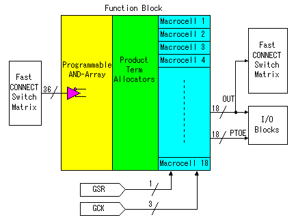 Function block is composed of the programmable AND array, product term allocator and macrocell. 36 pieces of signals inputted to the Function Block are divided into the true and complement signals by the programmable AND array and become 72 kinds of signals. In Product Term Allocator, it applys the signal with combination of them to the macrocell. A macrocell is composed of one D/T type flip-flop. The signals of set/reset/clock to this flip-flop are supplied by the Product Term Allocator. The output of the logic circuit can be connected with the pin without using a flip-flop, too. There are 18 independent macrocells in one Function Block. There are 18 pieces of output in the Function Block and they are connected with FastCONNECT Switch Matrix and I/O blocks. Also, the set/reset signal(GSR : Global Set/Reset) and the clock signal(GCK : Global Clocks) are inputted to the Function Block and are used for the condition of the operation of the flip-flop according to need. PTOE(Product Term Output Enable) signal is output to I/O block from Product Term Allocator. The number of the Function Blocks depends on the device. As for XC9536, 2 blocks are mounted, as for XC9572, 4 blocks are mounted and as for XC95108, 6 blocks are mounted. It isn't sometimes possible to use all macrocells by the limitation on the number of the pins. For details, confirm pin diagrams. There are few cases which connect all macrocells with the pin actually. Generally, there are macrocells to use only in the logic inside. 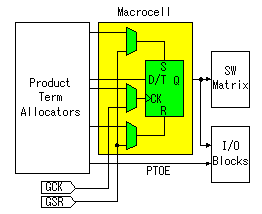 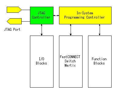 XC9500 devices are programmed in-system via a standard 4-pin JTAG(Joint Test Action Group) protocol. The devices fully support IEEE 1149.1 boundary-scan(JTAG). Because it is equipped with the pin for independent JTAG, the program can be changed as it mounted CPLD on the printed board. While programing, all input ports in the I/O block are set to the 'H' level. The wires to use in JTAG are the following four. Each use is shown below.
|
||||||||||||||||