Operation explanation
of the sine/cosine wave oscillator
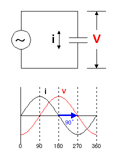 When adding an alternating current signal to the capacitor, the wave position (the phase) of the charging current of the capacitor and the voltage of the capacitor shifts by 90 degrees. The change of the voltage does the change to have been 90 degrees behind with the change of the charging current. 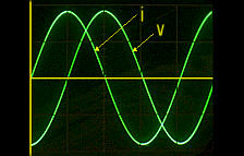 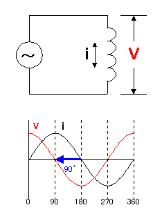 When adding an alternating current signal to the coil, it changes contrary to the capacitor. The change of the voltage moves ahead by 90 degrees with the change of the current. The circuit this time isn't using a coil. 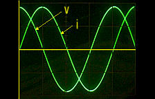
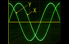
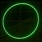
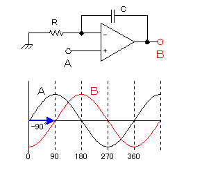 When a signal is inputted to the positive input terminal(Noninverting input) of the operational amplifier, the operational amplifier tries to output an in-phase signal as the output. However, because there is a capacitor, the output of the operational amplifier becomes the charging current of the capacitor. When a signal is inputted to the positive input terminal(Noninverting input) of the operational amplifier, the operational amplifier tries to output an in-phase signal as the output. However, because there is a capacitor, the output of the operational amplifier becomes the charging current of the capacitor.The change of the voltage of the capacitor does the change to have been 90 degrees behind with the change of the charging current. Because it is, the output signal voltage of the operational amplifier becomes the signal to be 90 degrees behind from the input signal. 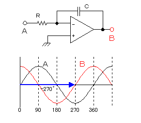 When a signal is inputted to the negative input terminal(Inverting input) of the operational amplifier, the operational amplifier tries to output the signal of the antiphase( 180° shifted signal ) as the output. Because it is 90 degrees behind in the voltage of the capacitor from the charging current, the output voltage of the operational amplifier becomes the signal to delay 270 degrees ( 180° + 90° ) from the input signal. 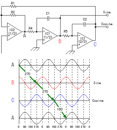 At the oscillation circuit which used an amplifier circuit, oscillation operation is done when the phase of the input signal of the amplifier and the phase of the signal which is fed back from the output are in-phase. The signal to have been 270 degrees behind is outputted when using a negative input terminal. The circuit which was made this time is using the two integration circuits of the negative terminal input. The phase difference of the input and the output of the two integration circuits shifts by the 540 degrees (180°) and only the integration circuit doesn't oscillate. Therefore, the loop of the oscillation is made by putting a operational amplifier (180°) of negative terminal input. This circuit becomes the circuit which is called "State variable-type activist filter" when it makes feed back the signal to the positive input of the IC2 from the B point. The photograph below is the wave form which observed the signal of each part, using the 4 channel adapter. It is the phase as the theory. 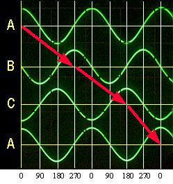 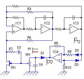 The blue part of the drawing on the left is the amplitude control circuit. In case of the operational amplifier, the control of the gain is generally done by the feedback to the negative input. However, this time, the negative input of the operational amplifier of the oscillation circuit is used for the oscillation operation. Therefore, it isn't possible to do usual gain control. The circuit this time controls the oscillation voltage by the feedback of the output of IC2 to the input of IC1. The output of IC2 is 90 degrees delayed than the negative input of IC1. When increasing the feedback from the output of IC2, the oscillation operation is suppressed. Because it is, it is possible to make do the oscillation operation which was stable if controlling the feedback in the oscillation voltage. The feedback is made both of the positive and the negative input of IC1. It is because the influence to the oscillation loop makes not become big. When there is not R3, the oscillation operation stops. I use the FET for the control of the feedback. To connect the sauce of the FET with the grounding, the feedback control is done with the positive terminal of IC1. I explain that the control circuit works below. As for the output of the oscillator, the negative DC voltage is made with the full wave rectified. This voltage is added to the gate of the FET and the resistance value between the drain and the sauce of the FET is changed. As for the operation of the FET, refer to "Operation explanation of the sine wave oscillator". The rectified DC voltage changes at the output voltage of the oscillator. The rectified negative voltage becomes big when the output voltage of the oscillator becomes big. Then, the resistance value between the drain and the sauce of the FET becomes big. With this, the feedback into the positive terminal of IC1 increases and the output of the oscillation decreases. The output voltage can be adjusted by the VR1. When the oscillation voltage becomes the power supply voltage, the signal tip is cut(Clip). It is necessary to adjust so as not to do the clip. 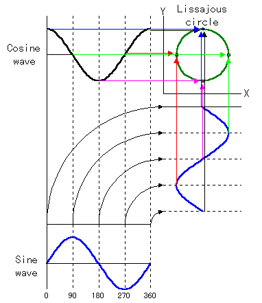 When inputting the cosine wave to the Y axis and inputting the sine wave to the X axis of the oscilloscope, the circular Lissajous diagram can be pictured. In case of the signal which doesn't have the distortion, the pictured circle becomes the true circle. You can confirm the distortion with the eyes. In this way, it doesn't understand the detailed distortion factor. To measure the correct distortion factor, the distortion factor meter is necessary. The photograph below is the one of the circuit which was made this time.
|