Figure 4.7 shows a half-wave rectifier circuit. The signal is exactly the top half of the input voltage signal, and for an ideal diode does not depend at all on the size of the load resistor.
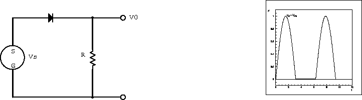
Figure 4.7: Half-wave rectifier and its output waveform.
The rectified signal is now a combination of an AC signal and a DC component. Generally, it is the DC part of a rectified signal that is of interest, and the un-welcomed AC component is described as ripple. It is desirable to move the ripple to high frequencies where it is easier to remove by a low-pass filter.
When diodes are used in small-signal applications - a few volts -
their behaviour is not closely approximated by the ideal model because
of the PN turn-on voltage.
The equivalent circuit model can be used to evaluate the detailed
action of the rectifier under these conditions.
During the part of the wave when the input is positive but less than
the PN turn-on voltage, the model predicts no loop current and the
output signal voltage is therefore zero.
When the input exceeds this voltage, the output signal becomes
proportional to ![]() , or about 0.6 V lower than the source
voltage.
, or about 0.6 V lower than the source
voltage.
The diode bridge circuit shown in figure 4.8 is a full-wave rectifier. The diodes act to route the current from both halves of the AC wave through the load resistor in the same direction, and the voltage developed across the load resistor becomes the rectified output signal. The diode bridge is a commonly used circuit and is available as a four-terminal component in a number of different power and voltage ratings.
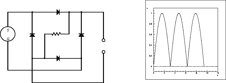
Figure 4.8: Full-wave rectifier and its output waveform.