The last component is of course the printed circuit board..
There are various ways to build the circuit which can be divided roughly into two classes, solder and non-solder The “ no soldering “ techniques are attractive initially but are really misleading for us starters as it can lead to intermittent contacts. Of course if we are a bit masochistic then we may spend a pleasant evening wondering which wire has fallen out or worse, which one is in it's hole but not making contact, or worst of all which wire is in a hole where it shouldn't be. Our main goal is making a working bike computer, not messing about with the connections.
Let's take the PCB route where everything has the connection planned and secure. Then we forget about that physical side of things and get on with the project.
To start making the PCB we need a few programs to get the project literally onto paper.
There are many very good schematic capture circuits, which number your components, adjust your drawing, anticipate the next stage which is the pcb layout…but they are also rather expensive.
We need something simpler which gives us the basic features, a program that allows us to draw the electrical circuit and number the components.
I used TinyCad. It is simple to learn but produces an excellent circuit diagram
The components are numbered and a list of materials generated, a parts list. As before, the program can be found on the internet and is FREE.
Below as an example our complete bike circuit and a list of the circuit components, generated by TinyCad.
====+ Parts List for Bk3.dsn +====
C1,C7 2 100n
C2,C3,C8 3 1uF
C4,C5 2 22p
C6 1 3uF
D2 1 IN4148
D1 1 LED
R1 1 100k
R3,R4 2 1k
R5 1 2k7
R2 1 300k
R6 1 390
S1,S2,S3 3
U1 1 VOLTREG
X1 1 XTAL 4 MHz
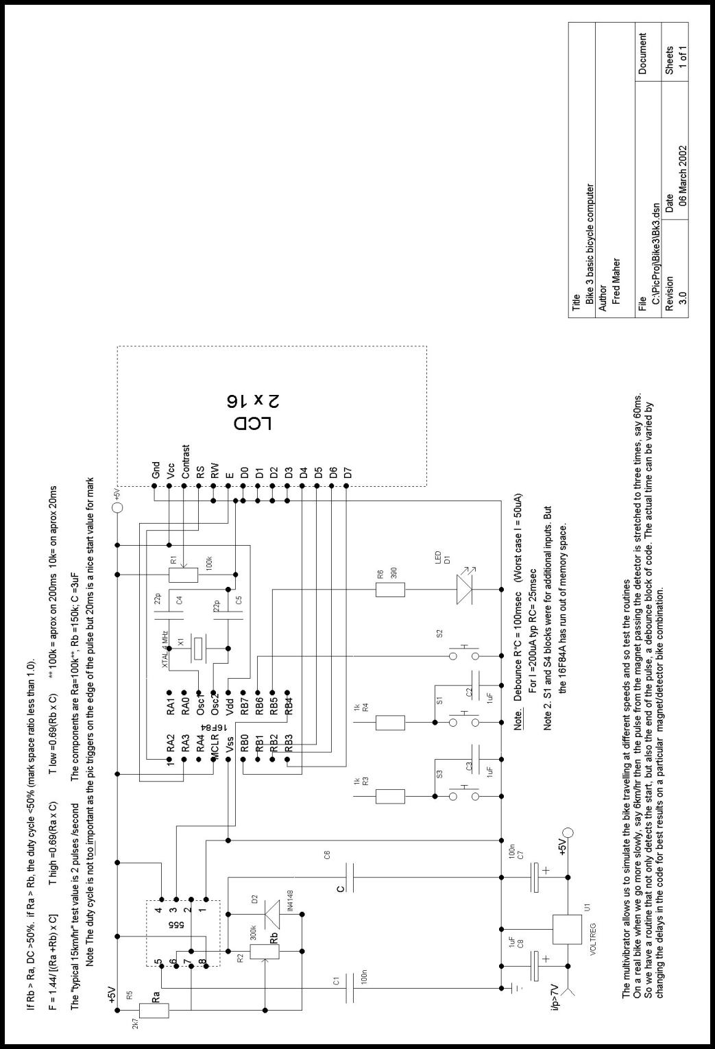
fig 5 the theoretical circuit of bike +dev system
We now need to make a physical circuit from the theoretical circuit of the Bike computer
Let's examine and talk about the layout below, and the step to make the PCB physically.
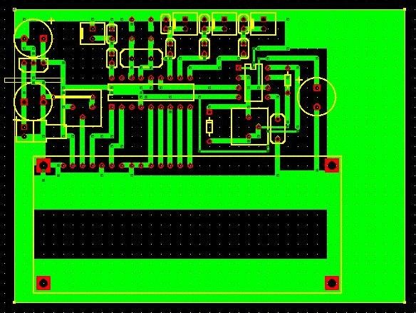
Fig.4 the pcb
The twin towers and the IC between them is the stabilized power supply. The long thin yellow IC outline is the PIC itself. Above the middle of the PIC, a rounded yellow rectangle is the 4Mhz xtal flanked by it's capacitors. To the left of the PIC, slightly down, a yellow square, the contrast potentiometer-. Finally occupying much of the bottom of the board, a large yellow rectangle with foursquare red fixing holes. The right most part which we will leave for later is the pulse generator, a 555.
For those of us who haven't seen a PCB , printed circuit board, it is a sheet of plastic covered with copper on one or on both sides. We are looking at the side with copper. It is coloured green. The other side has no copper. Each red dot represents a drill hole. Once all the little dots have been drilled. We can insert the components like the PIC into the top side, the side which is NOT green. Look at the PIC yellow outline. It has a V shape on the left edge., a big notch. This is to tell us where pin one of the integrated circuit is.
Pin1 is the first dot above the V ,the first dot in the top row of PIC pins. We count the pins CLOCKWISE from one, going right to nine, then we jump across to the other line of pins, still going clockwise and go left along the lower line of pins till we come to 18 at the top of the V once more, but now on it's bottom side. It is very important to understand this convention, so as to stick the components correctly into the waiting holes for soldering. Note if you look at the pins from the TOP side, they will now be numbered in an anti-clockwise direction, Think about this slowly and carefully.
The PCB TRACKS have been made as thick as possible. There are two reasons.
Thick tracks and wide earth zones mean good RF performance and heavy currents can be handled. Also soldering can be more ham-fisted before the tracks melt away.
The above PCB layout has been generated by a PCB program. This class of program can be very very expensive . Why? Well, it must be capable of producing a physical layout for the components, that reproduces all the dimensions to a fraction of a millimetre.
If this were not so, then automatic machinery which insert, or place components on the printed circuit board would probably place them with an offset. Then the next step, the flow solder bath, would solder the wrongly placed components with disastrous results. There would be many shorts between tracks and components.
We are not ( this time round) using SMD components. So our needs are not so stringent. But even so we need to be able to create the pads on the boards with sufficient accuracy to be able to insert the components without problems.
So? Well this time we are lucky as some PCB manufacturers give you a FREE professional program to design your PCB. They then manufacture it for you. There are standard prototype board sizes e.g. , 3.5 x 2.5 inch or 6 x 4 inch… many sizes. But for our project, this is not important,, we will use one of the smaller size boards.
This company which offers you the PCB generating program is called ExpressPCB. The program itself is called ExpressPCB The present version is V2.4 , but earlier ones will cover our needs perfectly . Most important, ExpressPCB. Exe is FREE.
Well using the program itself is very simple. But at this point we have to sit and study the controls. Once we have mastered the program we need to do the following.
We go to the component library and choose the component outlines of the components in the parts list generated with the TinyCad program. I used discrete resistors and capacitors . We can't expect to find a PIC in the library, but yes, there is an outline for an 18 pin DIP . This defines an IC with two rows of pin holes. The pins spaced 0.1” apart and the rows spaced 0.3” apart. I placed this about the middle of the board as the starting point. Of course as the other components are placed , we might find we are having to squeeze things together in one place, while in another the board is empty.
On an up market PCB program, you simply move the offending components, and the connecting tracks reroute themselves. In other words the tracks you have drawn to connect the components are not broken. Also these better class programs will advise you if your layout is wrong. What does wrong mean?
Many things, but at the simplest level say the theoretical diagram shows the junction of R3 and C1 connected to pin 3 of the PIC, but we have counted down the line of pins wrongly and connected to Pin5. . The sophisticated program will tell you it is wrong.
Of course at an even more sophisticated level, the PCB program will place all the components inside the board size you specify, generate all the interconnecting tracks and use as many layers as needed if it is possible.
But those programs are very expensive. We get no warning that R2 should be connected to PIN 7 instead of pin17. But we can make our own checks. We can take a copy of the theoretical circuit and starting, for example with the PIC, we CAN create the tracks which connect to the LCD. Below we have a cut out a chunk of the full PCB and have written the pin names on the connecting tracks for the DATA between the PIC and the LCD. You should look at this carefully and check it is correct against the theoretical circuit diagram. Check that each track joins the correct pin number of the 16F84A to the corresponding LCD pin number. Once all pins have been checked, then we are ready to go to the next stage
In the process of making the PCB .
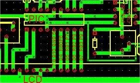
fig4b track connection detail
For Each track that you draw on the PCB…. Mark it's beginning and end on the theoretical electrical drawing with a fluorescent marker pen.
When you have finished creating all the tracks on the PCB, there MUST NOT be any unmarked lines on the schematic drawing. They must coincide, all lines must have the corresponding PCB track, otherwise there are errors.
Before leaving the pcb layout ( made with the Expresspcb program). Go back to fig4 the complete PCB layout drawing. There are two things wrong. Can you spot them?
Well the first thing would be fatal unless we know how to handle it. We have drawn the connections with the PIC pins numbered in an anticlockwise direction. We said earlier that this is the copper side of the board, and here you count the pins in a clockwise direction. Well maybe this is all a bit much to reason quickly, you need good special vision. But no panic. We carry on to the next stage where we will be transferring this image onto a clear acetate sheet. The program we will use, can FLIP the image so that we have the mirror image of fig4. This means that the bottom side pins are once again correctly positioned and go clockwise. Don't believe me? Look at fig.4 on your monitor. Then look at it's reflection in a mirror. I hope that convinces.
Why bother if it easy to solve? Well it would be so easy as well to overlook this little quirk of the Expresspcb program. Maybe there is a submenu command somewhere to flip the circuit , but I haven't found it.
The second thing is a typical chicken and egg situation. For one of a myriad of reasons modifications to the original design meant that the pcb was cut and chopped and hacked…( Note. this is possible because our PCB circuit has very wide tracks and they can take a lot of punishment)… and pin connections reassigned. So the working circuit now does not agree with the theoretical diagram. Which one is right?
Here I am to blame. It is quick and easy to update the modifications to a circuit diagram, not so quick and easy to generate a new PCB layout. Compare the PCB fig.4 with the electrical diagram fig.3 and locate the differences. They are all associated with the port connections to the PIC and the output from the pulse generator.
The main reason for the changes was that ( as we will see later) that a green LED is a great help in confirming not only that the wheel pulses are getting to the PIC, but that the PIC is processing them and is looping correctly.
Later we will come to a NEW version of the PCB that corresponds to the theoretical electrical drawing, line for line, track for track.
We are now in a position to actually make the PCB.
A word on the print process itself. We have to get our PCB track drawing onto a piece of clear acetate sheet. It will look like a large photographic negative, because it will be exactly scaled 1:1.
We go through the following basic steps to achieve this.
- Export the drawing from ExpressPCB to a drawing program say Photoshop.
- Use Photoshop to FLIP the drawing so that the pins go round clockwise,
- Use Photoshop print preview controls to adjust the pcb layout size to 1:1.
- Insert into your printer a clear DIN A4, or equivalent , clear THIN, acetate sheet
- Print the PCB drawing onto the acetate sheet. Let the printed ink dry for maybe two or three hours. ( paper dries immediately, but the acetate doesn't)
That is it, we are ready for the next step after a few words on what we have just done.
It is too much to expect that the PCB dimensions after passing between two programs and then onto a printer … It doesn't have to be laser, I use an HP710C … will come out exact first time. As the acetate sheet is rather expensive in my neck of the woods, I simply print the first trial run onto plain paper. Next I measure the length of the rows of pins where the PIC will go, to see that they are spaced exactly 0.1 “ apart. We don't even need a ruler., because we can place the PIC chip itself on our paper print out.
The first time we try this, probably the pins and marks won't coincide.. The first two or three pins will, but then we may notice that the pins are gradually separating from their marks the further along the row we go, landing on the spaces between the outline's pin marks. So we go back to step 3 above and adjust in the direction that is needed. How much adjustment? Well I sometimes have to scale up to 103% to get a printout where the pins coincide with the marks.
When the pins coincide exactly with the chip's paper outline, then we can do the next print on the acetate sheet.
Other print problems
Any other problem? Yes, the acetate sheet itself! It should be thin, not those thick chunky ones. Can we use a thick sheet? Yes, but if your printer is like mine, the sheet goes into the printer , over a roller and does a U turn , and comes out the front again. Some thick sheets won't bend.
Thick sheets have another problem. If we have managed to get the PCB tracks correctly onto them, then when we place the sheet over the photo sensitive plate to expose it, the lines will be fuzzy. This does not happen to the same extent with a thin sheet of acetate.
Do I hear you say but it does happen.! Indeed sir, you are correct. We would have to turn the track drawing over so that is against the photosensitive plate.
You say again, but if we turn the sheet over, the pins will be the wrong way round, anticlockwise.
Yes sir that is correct … a pause as we gradually realise that the anticlockwise output from the ExpressPCB program was exactly what we needed. Our apologies to the wise men in ExpressPCB.
So we need to go back to point two above and remove the word FLIP.
Nothing serious, except that ExpressPCB does not let you produce an image file suitable for a drawing program to handle. There is no bmp nor jpg, nor tiff nor similar outputs. Just a native format for processing the drawing in their factory, logically.
I get round this by printing to the printer, but not the HP printer a fax driver .
The fax program lets you preview before sending. And HERE you can save the preview as a bmp, tif, dcx image format any will do. The fax route is nice because it gets rid of the colours and turns everything into black and white, which is what we need for the acetate sheet.
So MY complete process to get the tracks on to acetate sheet , yours maybe similar or better, has the following steps:
- Export the drawing from ExpressPCB to a fax printer driver
- Re-export a bmp image to the drawing program, IrfanView
- Use IrfanView to get rid of speckle dots ( PCB grid )
- Use IrfanView print controls for setting 1:1 scale (100)
- Do trial print on paper.
- Place PIC on it's outline. Compensate if necessary
- Print onto acetate sheet. Let dry 3 hours
- Turn the acetate sheet over so that the ink is directly against the photosensitive plate.
That is it. Well I sneaked in a program called IrfanView. It has all the bells and whistles we need, and….. yes it is FREE. Find it on the internet, using the program name IrfanView. It is not too big and downloads quickly
WARNING Chemicals WARNING
The chemicals we are going to use are CAUSTIC and AT ALL TIMES YOU MUST KEEP THEM AWAY FROM THE CHILDREN.
- The developer is caustic soda, NaOH
- The etcher is Ferric Chloride, FeCl3
Caustic soda is not poisonous but it's great affinity for water can cause serious burns in contact with the skin. or being swallowed
If it gets into your eye, IMMEDIATELY wash you eye with abundant water for at least 5 minutes then get medical attention to check for damage. The prompt treatment is essential, to avoid permanent injury.
If in spite of the WARNING above, the kids get hold of it and swallow it, then YOU are really in trouble. You must take immediate action. Do the following.
- Call an ambulance or doctor
Explain if they have swallowed crystals or the dilute solution we are going to use.
Describe the symptoms and act immediately on instructions.
If it is not possible to get to a doctor or hospital then you must determine if the crystals or the dilute solution has been swallowed.
CRYSTALS: See if there are burn marks round the MOUTH. Administer 15cc/kg body weight of water or milk if possible. Rinse the mouth with abundant cold water, GET MEDICAL HELP AS SOON AS POSSIBLE
DILUTE SOLUTION: we use A 0.7gm/liter. Solution. This is not so bad as the crystals when swallowed, but it needs IMMEDIATE treatment.
As before immediately drink water or milk , 15cc/kg body weight , and rinse mouth abundantly with water Even though this is a dilute solution it is caustic and the child should GET MEDICAL HELP AS SOON AS POSSIBLE.
Ferric Chloride
This at first sight is worse as it eats away many metals. But it has an awful taste , a foul smell and it is most unlikely that a child would swallow the stuff. The main danger then is that it is CORROSIVE and it will stain your clothes, your skin a brownish yellow colour. The skin stain will go away after a few days, but the clothing is usually ready for the dustbin.
If it gets in your eyes, or hands wash with abundant water for at least five minutes then get immediate medical help
Waste elimination
There are many legislations locally in force for chemical disposal. You should consult before flushing these or any chemical down the toilet.


