 |
 | Positive exposure printed board |
| |
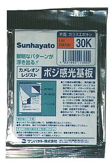
I use one side copper foil type glass epoxy board with being made by the Sunhayato company.
The model is 30K (Size 1.6mm x 75mm x 100mm).
Because it is the size which is bigger than the circuit to make(50 x 70), I've cut in the half.
When cutting the board, the ultraviolet rays of the sunlight or the fluorescence light do in the place not to irradiate.
|
|
| Mask pattern |
|
|
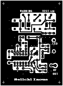
I use the mask pattern which was made in Visio.
It prints and it uses the mask pattern for the OHP sheet.
The + mark in the four corners shows the position of the corner of the PCB.
Make for the mask pattern to leave the copper foil as much as possible.
There is little copper to dissolve at the time of the etching.
This depends on the circuit to make.
You can download in the Visio file with the following link.
The file is the self extract-type compressed file. The downloaded file is extracted by the double-click.
The file named tounan.vsd (78.5KB) is made.
This is the file of the Visio exclusive use. The application program of Visio must be installed in your PC.
I made it in Visio 4.1. Of course, the file can do the editing in Visio.
The compressed file became bigger than the file before the compression.
Because it wasn't sometimes possible to download in case of not being the exe form, I did to the self extract type.
When printing the mask pattern to the OHP sheet with the printer, specify and print the best quality. In the dapples condition, it isn't possible to make the printed board successfully.
Because the pattern crushes, don't use the gif file of the figure on the right.
|
|
| Parts mounting drawing |
|
|
It is convenient when making the parts mounting drawing at the same time when picturing the mask pattern.
When picturing the pattern, you decide the parts mounting position. However, you sometimes get not to know a position of parts mounting.
Therefore, the parts mounting drawing becomes necessary.
|