 Clock control program Clock control program
 Modification of the macro program Modification of the macro program
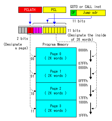
The program memory capacity of 16F series is a maximum of 8K words and they are divided into four pages every 2K words.These pages are specified with the value of the bit 3 and bit 4 of PCLATH register.
PIC16F873 are used for the Radio Controlled Clock introduced on other pages. The program memory of 873 is 4K words so the program memory is 2 pages. Therefore, the macro program for the page change is also only 2 pages control.
In PIC16F877, 8K words are mounted. And the additional program is allocated on the page 2. Therefore, the macro program for the page change is changed for 4 pages.
picmac1.inc
082
083
084
085
086
087
088
089
090
091
092
093
094
095
096
097
098
099
100 | setpch macro
if ($ >= 0) && ($ < 0x800)
bcf PCLATH,3
bcf PCLATH,4
else
if ($ >= 0x800) && ($ < 0x1000)
bsf PCLATH,3
bcf PCLATH,4
else
if ($ >= 0x1000) && ($ < 0x1800)
bcf PCLATH,3
bsf PCLATH,4
else
bsf PCLATH,3
bsf PCLATH,4
endif
endif
endif
endm |
A macro program is allocated to the program memory by assembling. Although the old macro program was operating only the bit 3 of PCLATH, this macro program operates bit 3 and bit 4. Therefore, the amount of the memory used is 1 word more than before. If a macro program is used 20 times, a program memory will be used 40 words. As a result of actually assembling, the existing program exceeded the page 1. Therefore, a part of initialization processing was moved to the page 2.
The example by which the macro program was developed on the page 2 is shown below. 2 words in red are allocated on the program memory.
0E38   118A 160A 2000 03855         LCALL   LED_DISP        ;Display 7 seg LED
                      03856         SETPCH                  ;
                          M         IF      ($ >= 0) && ($ < 0X800)
                          M         BCF     PCLATH,3
                          M         BCF     PCLATH,4
                          M         ELSE
                          M         IF      ($ >= 0X800) && ($ < 0X1000)
0E3B   158A               M         BSF     PCLATH,3
0E3C   120A               M         BCF     PCLATH,4
                          M         ELSE
                          M         IF      ($ >= 0X1000) && ($ < 0X1800)
                          M         BCF     PCLATH,3
                          M         BSF     PCLATH,4
                          M         ELSE
                          M         BSF     PCLATH,3
                          M         BSF     PCLATH,4
                          M         ENDIF
                          M         ENDIF
M ENDIF |
Allocation of General Purpose Register (GPR)
The specification of GPR differs in PIC16F873 and PIC16F877.
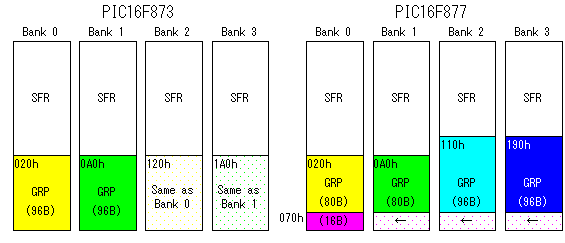
In case of 877, the last 16 bytes are common to all the banks. Then, the allocation of clock information was changed into the last 16 bytes. Thereby, these information can be read on any bank. The contents of the bank 0 are not changed. Only the allocation was changed. Therefore, it is uninfluential to the existing processing. The following 16 bytes were allocated to common area.
adr
070
071
072
073
074
075
076
077
078
079
07A
07B
07C
07D
07E
07F |
dec_sts1                ;decode status1
tm_ndh                  ;Day counter (Upper)
tm_ndl                  ;Day counter (Lower)
tm_10y                  ;10th of years counter
tm_1y                   ;1st of year counter
tm_10mth                ;10th of mounths counter
tm_1mth                 ;1st of mounth counter
tm_10d                  ;10th of days counter
tm_1d                   ;1st of day counter
tm_10h                  ;10th of hours counter
tm_1h                   ;1st of hour counter
tm_10m                  ;10th of minutes conuter
tm_1m                   ;1st of minute counter
tm_10s                  ;10th of seconds counter
tm_1s                   ;1st of second counter
tm_wd ;Week counter |
To access memories other than common area, it is necessary to change a bank.
The left-hand side of a left list shows the memory address. In other lists, the number of lines of a source code is shown. However, in this list, the memory address is written in order to explain the allocation of a memory.
Bank 2 can be used from 110h address. However, in this case, in order to make it the same position as bank 0 and bank 1, it is allocated from 120h. It is not so meaningful. GPR of bank 3 is not used.
The bank 1 and the bank 2 are allocated from 0A5h and 125h. As for this, refer to "It doesn't work normally when using the GPR of bank 1 and bank 2 from the head." of troubleshooting.
Change of the existing software
 Change of configuration word Change of configuration word
0016
0017
0018
0019
0020
0021
0022 | __config h'3F32' ;OSC is HS
;RB3,RB6,RB7 are I/O
;Brown-out detection OFF
;Power-up timer ON
;Code protection OFF
;Data code protection OFF
;Watchdog timer OFF |
The change point is to have stopped the brown-out detection function.
As for this, refer to "The CPU stops when making battery drive." of troubleshooting.
Bit allocation change of PORTC
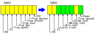 The use of each bit of PORTC was changed. The use of each bit of PORTC was changed.
The green bits are the changed bits.
The following source codes are changed in connection with this.
0117
0118
0119
0120

0128

1095

1136

1151

1219

3436

3963

3986

4077 | ;#define minute_out portc_buf,2 ;True minute output @@(Delete)
;#define hour_out portc_buf,3 ;True hour output @@(Delete)
;#define day_out portc_buf,4 ;True day output @@(Delete)
;#define month_out portc_buf,5 ;True month output @@(Delete)
-----------------------------------------------------------
;#define tco_out portc,0 ;Time code output @@(Delete)
-----------------------------------------------------------
; bsf minute_out ;Yes. Set true minute LED bit @@(Delete)
-----------------------------------------------------------
; bsf hour_out ;Yes. Set true hour LED bit @@(Delete)
-----------------------------------------------------------
; bsf day_out ;Set true day LED bit @@(Delete)
-----------------------------------------------------------
; bsf month_out ; Set true month LED bit @@(Delete)
-----------------------------------------------------------
movlw b'11000001' ;RC6(TX),RC7(RX),RC0(PW) input mode @@(Change)
-----------------------------------------------------------
movlw b'00110101' ;Set clear pattern @@(Change)
-----------------------------------------------------------
; bsf tco_out ;Set TCO LED ON (RC0) @@(Delete)
-----------------------------------------------------------
; bcf tco_out ;Set TCO LED OFF (RC0) @@(Delete) |
Deletion of unnecessary processing
Because the program memories of a page 1 ran short, deletion of unnecessary processing was performed and some changes were made.
3885
3886
3887
3888

4202
4203
4204
4205
4206
4207

4219
4220
4221
4222
4223
4224

4239
4240
4241
4242
4243
4244
4245 | ; movf tm_1s,f ;No. Read 1st of second @@(Delete)
; jpnz clock_main3 ;If 1st of second != 0, jump to clock_main3 @@(Delete)
; movf tm_10s,f ;Read 10th of second @@(Delete)
; jpnz clock_main3 ;If 10th of second != 0, jump to clock_main3 @@(Delete)
-----------------------------------------------------------
; clrf rep_cnt ;Clear key repeate counter @@(Delete)
; movf ikey_dat,w ;Read key number @@(Delete)
; rbank0 ; @@(Delete)
; movwf key_dat ;Save key number @@(Delete)
; bsf key_sts,0 ;Set key status @@(Delete)
; goto int_vec1 ;Jump to return @@(Delete)
-----------------------------------------------------------
goto kswchk5 ; @@(Add)
; clrf rep_cnt ;Clear key repeate counter @@(Delete)
; movf ikey_dat,w ;Read key number @@(Delete)
; rbank0 ; @@(Delete)
; movwf key_dat ;Save key number @@(Delete)
; bsf key_sts,0 ;Set key status @@(Delete)
; goto int_vec1 ;Jump to return @@(Delete) |
Initialization processing subroutine
In initialization processing, various kinds of register setup and initialization of GPR are performed. The initialization processing is in the page 1 of the program memory. However, it exceeded the capacity of page 1 when the area which was additional this time was initialized. Therefore, the part of the initialization processing was shifted to page 2 as the subroutine. The title is the initialization of bank 1 but the memory of bank 2 is initialized too.
Because it is the subroutine which exceeded a page, it is rewriting PCLATH by the setpch macro when returning.
3477
3478

4704
4705
4706
4707
4708
4709
4710
4711
4712
4713
4714
4715
4716
4717
4718
4719
4720
4721
4722
4723
4724
4725
4726
4727
4728
4729
4730
4731
4732
4733
4734
4735
4736
4737
4738
4739
4740
4741
4742
4743
4744
4745
4746
4747
4748
4849
4750
4751
4752
4753
4754
4755
4756
4757
4758
4759
4760
4761
4762
4763
4764
4765 | lcall bank1_init ;Bank1 data initialization @@(Add)
setpch ; @@(Add)
-----------------------------------------------------------
;@@@@@@@@@@@@@ Bank1 data initialization Subroutine @@@@@@@@@@@@@@@@@
bank1_init
rbank1 ;Set bank 1
clrf int_cnt ;Clear 100uS interval counter
clrf int_cnt10m ;Clear 10mS interval counter
clrf int_cnt100m ;Clear 100mS interval counter
clrf tco_cnt ;Clear TCO counter
clrf tco_hicnt ;Clear TCO high counter
clrf tco_period ;Clear TCO period counter
clrf tco_sts ;Clear TCO status
clrf sync_cnt ;Clear Sync valid counter
clrf ikey_dat ;Clear Key number
clrf ikey_dat0 ;Clear Key scan position
clrf ikey_dat1 ;Clear Key input data
clrf key_phs ;Clear Key phase
clrf rep_cnt ;Clear key repeate counter
clrf led_10y ;Clear LED 10th of year
clrf led_1y ;Clear LED 1st of year
clrf led_10mth ;Clear LED 10th of month
clrf led_1mth ;Clear LED 1st of month
clrf led_10d ;Clear LED 10th of day
clrf led_1d ;Clear LED 1st of day
clrf led_10h ;Clear LED 10th of hour
clrf led_1h ;Clear LED 1st of hour
clrf led_10m ;Clear LED 10th of minute
clrf led_1m ;Clear LED 1st of minute
clrf led_10s ;Clear LED 10th of second
clrf led_1s ;Clear LED 1st of second
clrf led_wd ;Clear LED week of the day
movlw seg7_ha ;Set pattern table head address
movwf led_ha ;Save pattern table head address
movlw seg7_0 ;Set pattern 0
movwf led_0 ;Save pattern 0
movlw seg7_1 ;Set pattern 1
movwf led_1 ;Save pattern 1
movlw seg7_2 ;Set pattern 2
movwf led_2 ;Save pattern 2
movlw seg7_3 ;Set pattern 3
movwf led_3 ;Save pattern 3
movlw seg7_4 ;Set pattern 4
movwf led_4 ;Save pattern 4
movlw seg7_5 ;Set pattern 5
movwf led_5 ;Save pattern 5
movlw seg7_6 ;Set pattern 6
movwf led_6 ;Save pattern 6
movlw seg7_7 ;Set pattern 7
movwf led_7 ;Save pattern 7
movlw seg7_8 ;Set pattern 8
movwf led_8 ;Save pattern 8
movlw seg7_9 ;Set pattern 9
movwf led_9 ;Save pattern 9
movlw seg7_a ;Set hyphen pattern
movwf led_a ;Save hyphen pattern
movlw seg7_b ;Set OFF pattern
movwf led_b ;Save OFF pattern
rbank2
clrf led_hyphen ;Clear LED hyphen
clrf led_cnt100u ;Clear LED 100us counter
clrf led_wkdata ;Clear LED work data
rbank0 ;Set bank 0
return |
When calling a subroutine beyond the page, "lcall" is used. "lcall" is one of the directives and is not the instruction of PIC itself. It is developed by the following 3 steps by assembling. Before a call instruction is executed, processing which sets up the value of PCLATH is performed.
        bcf     pclath,3
        bsf     pclath,4
        call    bank1_init
LED display program subroutine call
LED display processing is added to the processing executed for every second. The added processing is subroutine form.
3855
3856 | lcall led_disp ;Display 7 seg LED @@(Add)
setpch ; @@(Add) |
Additional program
From here, it is the main software of this project.
PORTD and PORTE
A setup of PORTD and PORTE which can be used by PIC16F877 is added. 877 was adopted to use these ports.
3422
3423

3438
3439 | clrf PORTD ;Clear PORTD @@(Add)
clrf PORTE ;Clear PORTE @@(Add)
-----------------------------------------------------------
clrf TRISD ;RD7-0:output mode @@(Add)
clrf TRISE ;RE2-0:output mode @@(Add) |
7 segment data
These are the definitions of 7 segment data corresponding to the number.
0155
0156
0157
0158
0159
0160
0161
0162
0163
0164
0165
0166
0167 | ;@@@ 7 segment LED data
seg7_0 equ b'00111111' ;-gfedcba Pattern 0 @@(Add)
seg7_1 equ b'00000110' ; Pattern 1 @@(Add)
seg7_2 equ b'01011011' ; Pattern 2 @@(Add)
seg7_3 equ b'01001111' ; Pattern 3 @@(Add)
seg7_4 equ b'01100110' ; Pattern 4 @@(Add)
seg7_5 equ b'01101101' ; Pattern 5 @@(Add)
seg7_6 equ b'01111101' ; Pattern 6 @@(Add)
seg7_7 equ b'00000111' ; Pattern 7 @@(Add)
seg7_8 equ b'01111111' ; Pattern 8 @@(Add)
seg7_9 equ b'01101111' ; Pattern 9 @@(Add)
seg7_a equ b'01000000' ; Hyphen @@(Add)
seg7_b equ b'00000000' ; OFF @@(Add) |
GPR
The memory definition used this time is added to GPR.
led_ha is the area which stores the address of led_0. When reading and writing a memory using the indirect addressing processing(FSR/INDF), it uses an address at the head of the table. The processing becomes more easily, recording an address at the head of the table beforehand.
led_0 to led_b are the area which records LED 7 segment data. These areas are provided to use indirect addressing processing too.
led_10y to led_wd are the area which stores clock information. In the existing software, clock information is stored with a label called "tm_xx". The time of "tm_hour" is managed in 24 hours. In the processing this time, it converts into the display for 12 hours. Therefore, it is copying the information of "tm" to led_10y through led_wd. It is the limit that even this is allocated to bank 1. It is 80 bytes that are peculiarly allocated on bank 1. That is, it is to 0EFh. The address of led_wd is 0EEh. There is 1 byte leeway but it allocates the remainder on bank 2.
Immediately after the turning on, clock information isn't fixed. In this situation, it is making a hyphen blink to the LED. led_hyphen is the area which manages the state of the lighting-up/the turning-off.
led_cnt100 is the counter area to make 100 microseconds.
led_wkdata is the area which saves input in the subroutine which writes data in CPLD.
led_ff is the area which counts the number of times of a music skip after sounding a chime at the time of 0:00 on January 1.
led_fsr is the area which saves the value of FSR in CPLD write-in processing.
0169


0304
0305
0306
0307
0308
0309
0310
0311
0312
0313
0314
0315
0316
0317
0318
0319
0320
0321
0322
0323
0324
0325
0326
0327
0328
0329
0330
0331
0332
0333
0334
0335
0336
0337
0338
0339
0340
0341
0342
0343
0344 | ;*** Register area definition (bank 0)
[Skipping]
;@@@ Register area for 7 seg LED
led_ha ;Table head address @@(Add)
led_0 ;7seg pattern 0 @@(Add)
led_1 ;7seg pattern 1 @@(Add)
led_2 ;7seg pattern 2 @@(Add)
led_3 ;7seg pattern 3 @@(Add)
led_4 ;7seg pattern 4 @@(Add)
led_5 ;7seg pattern 5 @@(Add)
led_6 ;7seg pattern 6 @@(Add)
led_7 ;7seg pattern 7 @@(Add)
led_8 ;7seg pattern 8 @@(Add)
led_9 ;7seg pattern 9 @@(Add)
led_a ;7seg hyphen @@(Add)
led_b ;7seg OFF @@(Add)
led_10y ;10th of year @@(Add)
led_1y ;1st of year @@(Add)
led_10mth ;10th of month @@(Add)
led_1mth ;1st of month @@(Add)
led_10d ;10th of day @@(Add)
led_1d ;1st of day @@(Add)
led_10h ;10th of hour @@(Add)
led_1h ;1st of hour @@(Add)
led_10m ;10th of minute @@(Add)
led_1m ;1st of minute @@(Add)
led_10s ;10th of second @@(Add)
led_1s ;1st of second @@(Add)
led_wd ;Week of the day @@(Add)
endc
;*** Register area definition (bank 2) 80 bytes can be used
cblock ram_base2
led_hyphen ;0:Hyphen OFF, 1:Hyphen ON @@(Add)
led_cnt100u ;100us counter @@(Add)
led_wkdata ;LED work data @@(Add)
led_ff ;Fast forward data @@(Add)
led_fsr ;FSR save area @@(Add)
endc
seg7_ha equ led_0 ;LED pattern table head address @@(Add) |
Bank switching of GPR
In this project, GPR from bank 0 to bank 2 is used. When using banks other than a common bank, you have to change a bank if needed. Bank switching can be easily performed by using a macro program.
        rbank0     ;The macro changed to bank 0
        rbank1     ;The macro changed to bank 1
        rbank2     ;The macro changed to bank 2
picmac1.inc
54
55
56
57
58
59
60
61
62
63
64
65
66
67 | rbank0 macro ;register bank 0 select
bcf STATUS,5
bcf STATUS,6
endm
;
rbank1 macro ;register bank 1 select
bsf STATUS,5
bcf STATUS,6
endm
;
rbank2 macro ;register bank 2 select
bcf STATUS,5
bsf STATUS,6
endm |
A left list is a bank-switching macro program.
The bit 5 and bit 6 of a STATUS register are the bits for bank specification.
The macro program for bank 3 is also made. However, since it is not used this time, it is not mentioned to this list.
Allocation of the additional program
The allocating of an additional program is done from the page 2 of the program memory. Allocating is designated from 1000h by "org".
4307
4308
4309
4310
4311
4312 | ;@@@@@@@@@@@@@@@@@@@@@@@@@@@@@@@@@@@@@@@@@@@@@@@@@@@@@@@@@@@@@@@@@@@@
; 7 seg LED Display subroutine
; Author : Seiichi Inoue
;@@@@@@@@@@@@@@@@@@@@@@@@@@@@@@@@@@@@@@@@@@@@@@@@@@@@@@@@@@@@@@@@@@@@
org 0x1000
led_disp |
Check of a power supply state
4313
4314
4315

4655
4656
4657
4658
4659
4660 | rbank0
btfss portc,0 ;AC Power ON ?
goto led_off ;No. Jump to LED contro; OFF
-----------------------------------------------------------
;*** Display control OFF
led_off
clrf portd ;Clear PORTD
clrf porte ;Clear PORTE
bcf portc,5 ;Clear CK bit
return |
Even if AC power supply stops, CPU and a receiver operate continuously with a battery. However, in the case of a Radio Controlled Clock, time is displayed several minutes after a power supply becomes normal. When the battery is equipped, after AC power supply has become normal, time is displayed immediately. The state of AC power supply is checked on the voltage of +12V of a power supply unit. +12V is changed into +5V by the resistors, and is inputted into the bit 0 of PORTC. When this bit is "1", AC power supply is normal and LED display processing is performed. Since it is in the state which AC power supply has stopped when this bit is "0", LED display processing is not carried out, but carries out only processing which suspends the output to CPLD, and ends a subroutine. As for this, refer to "LED of a day of the week lights up thinly at the time of a battery drive." of troubleshooting.
Hyphen display at the time of time information un-acquiring
4316
4317
4318
4319
4320
4321
4322
4323
4324
4325
| rbank1
btfsc det_mark_1st ;1st marker detected ?
goto led_dsp03 ;Yes. Jump to time decode check
led_dsp01
rbank2
btfsc led_hyphen,0 ;LED hyphen ON ?
goto led_dsp02 ;Yes.
rbank1
movlw d'10' ;Read LED hyphen data
movwf led_10y ;Set 10th of year
[Hereinafter, skipping] |
Time information is not acquired immediately after switching on a power supply. Lapsed time is displayed on a time information storing memory(tm_xx) until normal time is obtained. These displays are not so meaningful. Then, the hyphen (G segment of seven segments) is blinked in the meantime.
If marker appearance is completed, det_mark_1st (bit 1 of dec_sts1) will be set to "1." Moreover, if decoding of time is completed, dec_time_1st (bit 4 of dec_sts1) will be set to "1."A hyphen is blinked when either of these two bits is "0." When these bits are "1", it means that normal time information was acquired and LED display processing is performed.Å@No.10 pattern code is used for a hyphen display.
Copy of time information
4366
4367
4368
4369
4370
4371
4372
4373
4374
| led_time_read:
movfw tm_10y ;Read 10th of year
movwf led_10y ;Save 10th of year
movfw tm_1y ;Read 1st of year
movwf led_1y ;Save 1st of year
movfw tm_10mth ;Read 10th of month
btfsc status,z ;10th of month = 0 ?
movlw d'11' ;Yes. Set LED OFF data
movwf led_10mth ;Save 10th of month
[Hereinafter, skipping] |
Time information (tm_xx) is copied to the memory for LED display processing. Conversion of time information is performed at this time. The acquired time information is 24 hours. Therefore, 13:00 is changed into 1:00 and 23:00 is changed into 11:00 like that. Since the information on the 10th place and the 1st place of time is separate, it is not simple. Moreover, LED is made to switch off when the 10th place of the month, the 10th place of a day, and the 10th place of time are "0." This is for conspicuousness. In order to switch off LED, No.11 pattern code is used.
Time signal control
4458
4459
4460
4461
4462
4463
4464
4465
4466
4467
4468
4469
| ;*** Time signal control
movlw d'6' ;Set 6 o'clock
subwf led_1h,w ;Check hour
btfss status,z ;6 o'clock ?
goto led_sig01 ;No.
goto led_sig07 ;Jump to True time check
led_sig01
movlw d'7' ;Set 7 o'clock
subwf led_1h,w ;Check hour
btfss status,z ;7 o'clock ?
goto led_sig02 ;No.
goto led_sig07 ;Jump to True time check
[Hereinafter, skipping] |
The time signal by a melody is sounded to 6:00, 7:00, 8:00, and 9:00. Since distinction of the morning and an afternoon has not been carried out, a time signal sounds 8 times per day. Eight kinds of melodies are mounted in the melody IC used this time. Therefore, the same melody sounds in the same time.
A chime is sounded to 0:00 on January 1, and the new year is told. Even when a chime is sounded, the counter of melody selection is updated. Therefore, a gap of a melody and time arises annually. In order to prevent this, melody IC is started 7 times for every second from 0:01 on January 1, and a melody selection counter is updated compulsorily. Thereby, time and a melody are synchronized. Since it is noisy when a melody sounds at this time, melody IC was made into silence mode and has been updated.
Time information output control
This is the processing to write the information the year, the month, the day, the day of the week, the hour, the minute and the second in the latch register of CPLD.Å@The position of a latch register is specified by a total of 4 bits of 3 bits of PORTE, and the bit 7 of PORTD.Å@7 bits of low ranks of PORTD are used for the output of time information. An output process is performed by Åhled_writeÅh subroutine. In this subroutine, number information is changed into the control information on seven segments, and is written in CPLD. Control of writing is performed by the bit 5 of PORTC. After setting all information as PORTD and PORTE, the bit 5 of PORTC is set to "1." In this state, it is not written in CPLD yet. The bit 5 of PORTC is set to "0" after 100 microseconds. Thereby, the information on seven segments set as PORTD is written in the latch register of CPLD. Until writing processing of next information, a 100 microsecond wait is placed. This is for securing the operating time of CPLD.
13 kinds of information is written to CPLD in all. Since it takes about 200 microseconds to write one information, the time taken to write all becomes about 3Å@milliseconds. This time is satisfactory as whole processing.
4558
4559
4560
4561
4562
4563
4564
4565
4566


4662
4663
4664
4665
4666
4667
4668
4669
4670
4671
4672
4673
4674
4675
4676
4677
4678
4679
4680
4681
4682
4683
4684
4685
4686
4687
4688
4689
4690
4691
4692
4693
4694
4695
4696
4697
4698
4699
4700
4701
4702 | ;*** Display control
led_cont
rbank0
movlw b'00000011' ;Set 10th of year selector
movwf porte ;Set selector data
rbank1
movlw b'10000000' ;Set 10th of year selector
iorwf led_10y,w ;Set data
call led_write ;Write data
[Skipping]
;@@@@@@@@@@@@@@@@@@@@ Data write Subroutine @@@@@@@@@@@@@@@@@@@@@@@@@
led_write
rbank2
movwf led_wkdata ;Save input data
movfw fsr ;Read FSR
movwf led_fsr ;Save FSR
movlw b'00001111' ;Set mask
andwf led_wkdata,w ;Pickup LED data
rbank1
addwf led_ha,w ;LED pattern table HA + LED data
movwf fsr ;Set table address
movfw indf ;Read 7seg data
rbank0
movwf portd ;Set 7seg data
rbank2
movfw led_fsr ;Read saved FSR
movwf fsr ;Recover FSR
movlw b'10000000' ;Set mask
andwf led_wkdata,w ;Pick up selector data
rbank0
iorwf portd,f ;Set selector data
bsf portc,5 ;Start clock pulse
rbank2
call led_t100u ;100usec wait
rbank0
bcf portc,5 ;Stop clock pulse (Data latch)
rbank2
call led_t100u ;100usec wait
rbank0
return
;@@@@@@@@@@@@@@@@@@@ 100usec Timer Subroutine @@@@@@@@@@@@@@@@@@@@@@@
led_t100u
movlw d'63' ;Set loop cnt
movwf led_cnt100u ;Save loop cnt
led_t100ulp
nop ;Time adjust
nop ;Time adjust
decfsz led_cnt100u,f ;cnt100u - 1 = 0 ?
goto led_t100ulp ;No, continue
return |
|