Circuit explanation of RCC with LSD
|
A part of this page is the same as the Radio Controlled Clock introduced on another page.
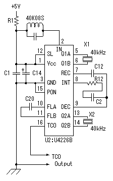 In the case of Japan, the radio of standard time is transmitted as long wave radio from the transmitting station in OOTAKADOYA mountain (40kHz) of Fukushima Prefecture, and HAGANE mountains (60kHz) of Nagasaki Prefecture. Reception of this radio is performed by U4226B. The parts attached outside are a receiving coil, 40kHz crystal oscillators, and some resistors and capacitors. U4226B is designed for radio-controlled clock applications in the frequency range of 40 to 80 kHz. Refer to the data sheet for detailed specification. 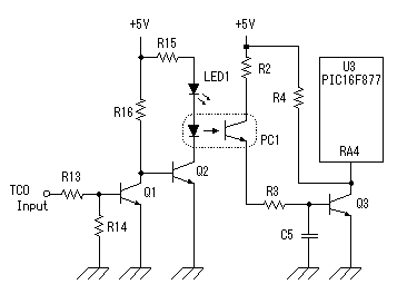 The output signal TCO( Time Code Output ) of U4226B is the pulse of 0V to 5V. This signal is amplified by the transistors in order to make sharp the rising edge and the falling edge of the pulse. LED1 is for the monitors of a TCO signal. The time information sent by radio consists of 60 pulses, and one pulse is sent in 1 second. Although the width of each pulse changes with information sent, blink of LED1 is performed for every second. Thereby, you can check whether radio has received normally. A receiver and a display processor can be installed in the place left by cable splicing. In this case, noise may be induced to a cable. The receiver circuit and the display processing circuit are electrically separated by the photo coupler (PC0) in order to lessen the influence. The capacitor C21 connected to the base of Q3 is for removing the noise induced to the cable. If the capacity of this capacitor is large, pulse shape will deteriorate. A TCO signal is inputted into RA4 port of PIC16F877. Unlike other ports, this port is an open drain type. That is, a pull-up (it pulls up to +5V) is not carried out inside PIC. Therefore, the pull-up is carried out by R4. 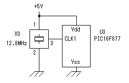 The time of this clock is displayed by the time information sent on radio. The right time cannot be displayed if radio stops. Therefore, the highly precise crystal oscillator is used for the clock of PIC. Oscillation frequency is 12.8MHz. The execution time of one step of PIC becomes 4/12.8 = 0.3124 microseconds. When radio is received normally, the accuracy of this oscillator does not become a problem. Two or more equipment, such as a cesium beam type atom frequency standard machine, is used for the Japanese standard clock. The accuracy is announced as 10-13. Since it is 31,536,000 seconds for one year, it is the accuracy that the error for 1 second will arise in 317,098 years. This system is not used so long. Therefore, this is the clock which does not go wrong at all. The time of this clock is displayed by the time information sent on radio. The right time cannot be displayed if radio stops. Therefore, the highly precise crystal oscillator is used for the clock of PIC. Oscillation frequency is 12.8MHz. The execution time of one step of PIC becomes 4/12.8 = 0.3124 microseconds. When radio is received normally, the accuracy of this oscillator does not become a problem. Two or more equipment, such as a cesium beam type atom frequency standard machine, is used for the Japanese standard clock. The accuracy is announced as 10-13. Since it is 31,536,000 seconds for one year, it is the accuracy that the error for 1 second will arise in 317,098 years. This system is not used so long. Therefore, this is the clock which does not go wrong at all. Although time is displayed by LED, the display circuit by LCD is also prepared. However, it is incorporated in the case so it is not usually visible. It is very effective for the check of a clock of operation. The display of the LCD becomes reference when LED does not operate normally by the fault of software. Although time is displayed by LED, the display circuit by LCD is also prepared. However, it is incorporated in the case so it is not usually visible. It is very effective for the check of a clock of operation. The display of the LCD becomes reference when LED does not operate normally by the fault of software.SC1602BSLB used this time has the 8-bit mode and the 4-bit mode as data transfer mode. In this circuit, the 4-bit mode is used on account of the control port. RB port is used for the control port of PIC. In order to control in the 8-bit mode, it is needed also except RB port. RS (Register Select) is the terminal for a change of a command register (L) and a data register (H). E (Enable Signal) is a terminal for making information read into LCD. DB4-7 are the terminals for information transmissions. Moreover, the contrast of the character displayed on LCD can be adjusted by Vo. All the terminals that are not used are connected to grounding. SC1602BSLB has a back light function but it was not used this time. RB port serves also as the key input port of a timer setup (it is not a time setup). RB port is used if needed, changing to the input mode and the output mode. 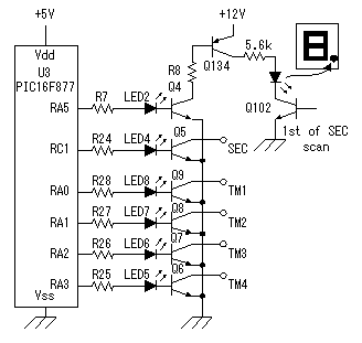 Lighting control of the LEDs which display the operating state and the control circuit of the external circuit are driven using RA ports and RC ports. Lighting control of the LEDs which display the operating state and the control circuit of the external circuit are driven using RA ports and RC ports.A receiving state is outputted to RA5. The dot LED of the 1st place of a second lights up by the output. Because the common cathode type is used for LED for a second display, a PNP transistor is needed for a drive. The signals of timer are outputted to RA3 from RA0. Although the external circuit is not connected with this equipment, an external circuit is controllable if needed. Because LEDs except a receiving state hide into a case, they are not usually visible.
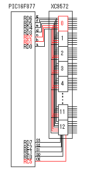 Processing overflow will be assumed if LED of a clock display is directly driven by PIC16F877. Therefore, only collection and the output of date time information are made to perform for every second in 877. And the latch register by CPLD is made to memorize those information. There are eight latch registers in one CPLD device. They are 16 latch registers in two CPLD. 13 of them are used for this circuit. Selection of a latch register is performed by RE0, RE1, RE2, and RD7. The control data of seven segments is outputted from RD0-RD6. Moreover, the writing to a latch register is performed when RC5 falls to "0" from "1." Display data is set as RD0-RD6, register selection data is set as RE 0-2 and RD7, and RC5 is set to "1." At this time, writing is not performed yet. When RC5 is made to "0", the writing to a latch register is performed. The reason RE port and RD port are together put as a control line of register selection is that the port was lacking. The software of this clock is using Radio Controlled Clock as the base. Then, in order to avoid change of the port currently used, the port of a control line became irregular. 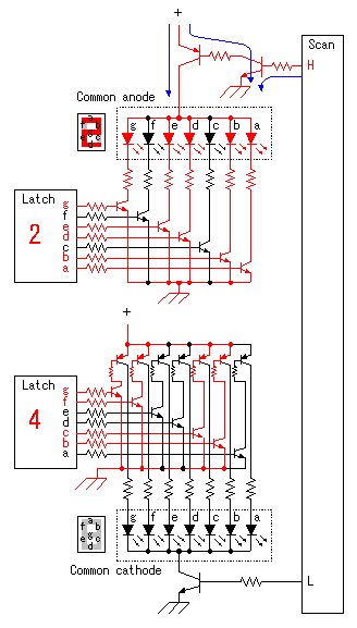 The left figure expresses operation of the drive circuit of LEDs. The upper one is the case of common anode type LED. This type of LED is used for the year, the month, the day, the hour and the minute. A lower one is common cathode type LED. This type is used for the second. I was going to make all the common anode type. However, I was not able to obtain the common anode type of a just right size. In fact, the bought type was a common cathode type. Display information is memorized by the latch register for every second like the above-mentioned explanation. Much current is needed if the light is switched on simultaneously. The maximum current of large-sized LED currently used for the hour and minute is 25mA per one segment in a direct-current drive. It is 175mA when the light is switched on simultaneously 7 segments. It is 700mA when four LED is turned on simultaneously. Because there is other LEDs, much more current flows. In order to make it power saving, LED is made to turn on in order at high speed, although power supply capacity does not have a problem. The circuit consists of two scanning groups. They are the scan (RA port) of six LEDs of the hour, the minute and the second, and the scan (RB port) of eight LEDs of the year, the month and the day. By this, the number of LED turned on simultaneously is two. In a common anode type case, a number is displayed by making into H level the drive circuit connected to the anode by PIC for a scan. A common cathode type is also the same and a number is displayed by making into H level the drive circuit connected to cathode by PIC for a scan. 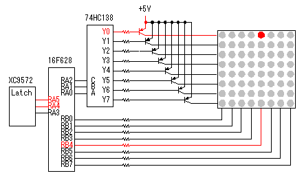 The LED matrix is used for the display of a day of the week. The day of the week information is recorded in a latch register as binary information, and it is transmitted to PIC16F628. The meaning of information is 0=Lights out, 1=Sunday, 2=Monday, 3=Tuesday, 4=Wednesday, 5=Thursday, 6=Friday and 7=Saturday. The LED matrix is used for the display of a day of the week. The day of the week information is recorded in a latch register as binary information, and it is transmitted to PIC16F628. The meaning of information is 0=Lights out, 1=Sunday, 2=Monday, 3=Tuesday, 4=Wednesday, 5=Thursday, 6=Friday and 7=Saturday.KANJI character display control is performed by PIC based on the information. 3-8 decoder of 74HC138 is controlled by a binary code, and a screen line is specified. The lighting-up information of the LED is output at the same time to the RB ports. A left figure is in the state which shows Friday. The screen line is controlled by the 1millisecond by PIC so you can see without flickering.  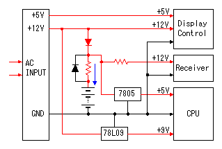 The power unit outputs the stable voltage of +12V and +5V from the input voltage of AC100V. The voltage is converted into the voltage which is necessary in each unit by the voltage regulator. Moreover, charge of the battery is performed through a resistor from the power supply of +12V. For about the charge, please look at "Adjustment of charging current". About 20mA current usually flows into +5V of the CPU unit. Considering only it, 100mA type 78L05 etc. is enough. However, when AC power supply stops, the current momentarily exceeding 100mA flows. Therefore, 1A type 7805 is used as a regulator. This cause is based on the circuit characteristic of CPLD used this time. For about this affair, please look at "LED of a day of the week lighting up thinly at the time of a battery drive".  When AC100V to the power unit stop, the power supply is supplied from battery. The circuit driven with battery is only the CPU circuit which carries out processing of the clock and the receiving circuit. The LED display circuit and the time signal circuit are not backed up. 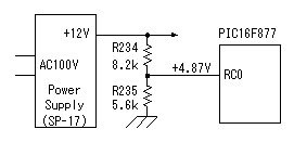 When AC power supply stops, the CPU and the receiving circuit are continuously operated with battery. However, if the power supply to CPLD of a display control circuit stops, the input voltage of CPLD will flow into a power supply circuit. In order to prevent it, a stop of AC power supply is detected by CPU, and the input to CPLD is suspended. In this circuit, the voltage of +12V was transformed into the voltage of about 5V by the resistor, and it has inputted into PIC. In PIC, when this port is 0V, it is recognized as a power supply stop and the output to CPLD is made to 0V. There is an output of +5V in the power supply. However, the CPU unit does not have the +5V wiring from the power unit. |