Processing explanation of signboard
;********************************************************
;
;             The signboard control processing
;
;                                 Author : Seiichi Inoue
;********************************************************
I wrote the title of the program using the comment( ; ).
        list            p=pic16f84a
        include         p16f84a.inc
The standard label definition of PIC16F84A is read by the INCLUDE directive. When using the standard definition of the Microchip Inc., a warning message about TRISA and TRISB is displayed. So, I modified the definition file. Definition files are generally installed in the place below. c:\Program Files\Mplab\p16f84a.inc
The change parts of the contents of p16f84a.inc are hereinafter. ; P16F84A.INC Standard Header File, Version 2.00'(modify) TRISA EQU H'0085' -> H'0005' TRISB EQU H'0086' -> H'0006'
__config _hs_osc & _wdt_off & _pwrte_on & _cp_off
When using a label for the operand of this command, the constant of the label must be defined beforehand. The labels which were specified this time are defined as follows at the standard label. _CP_OFF EQU H'3FFF' _PWRTE_ON EQU H'3FF7' _WDT_OFF EQU H'3FFB' _HS_OSC EQU H'3FFE'
__config h'3ff2'
;**************** Label Definition ******************** The definition of the label constant to use by the processing is done. The standard label of PIC16F84A is read in INCLUDE directive. There are a definition of the memory address and a definition of the data value in the label definition. They are defined using either of the EQU directive. In the list this time, I divided the EQU of the address and the EQU of the data setting to easiness understanding. ;************************ ;* Time adjust * ;************************ ;This data decides a scroll speed. Basic rate is 26msec. tm_adj equ 0c ;Time adjust(26msec x 12) ;************************ ;* EEPROM data size * ;************************ ;If the data size is 30 bytes, then simply set d'30'. e_size equ d'32' ;EEPROM data size ;*************** EEPROM Data Definition ***************
org h'2100'
de b'11111111'I used an EEPROM for the memory which holds the contents of the message to display. The data of the EEPROM specifies a memory address from h'2100'. Address h'2100' is h'00' at the EEPROM memory. The specification of the address is done by the ORG directive. Each bit means that the LED lights up in '0' and means that the LED goes out in '1'. ;**************** Program Start *********************** Instruction is executed from Zero addresses of the program memory when making the power ON of the PIC. When there is interruption processing, processing is begun from the addresse 4. It makes each processing jump with the GOTO instruction. ;**************** Initial Process ********************* The following processing is done as the initialization processing after the turning on.
;************** Screen Load Process ******************* Because a message is displayed on the LEDs of 128 (8 x 16), I am calling it a screen. The blink condition of 128 LEDs is controlled in 16 bytes of the RAM file memory. Because it is possible to do only the blink control of eight LEDs at the same time in PIC, the blink control of eight units is at high speed done. At the eyes of the person, it seems to be controlling 128 LEDs at the same time. The control begins with eight LEDs at the end of being rightmost and one row is shifted. If changing the contents of the RAM file memory, the lighting-up situation of the LED can be changed. The blink condition of eight LEDs is output to port B and a row control binary signal is output to 4 bits of port A(RA3-RA0).
In the rewriting processing of screen data, it has the processing to turn off an LED first. The LED of the following row has lit up by the data of the row in front when changing an LED to the following row without turning off it. ;************ Begin Interruption Process **************
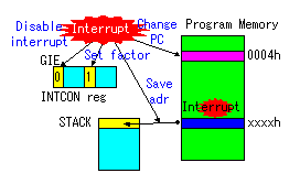
Next, it checks the kind of the interruption. This time, because it generates only time-out interruption, the checking is unnecessary. I am checking time-out bit (T0IF) for processing practice. When there is not a time-out bit and the interruption occurs, it is making jump to initialization processing. ;************ END of Interruption Process **************
The STATUS register is recovered first and the W register is recovered next. Because, the W register is used for recover process for the STATUS register. To do the W register in the recover, it is necessary the technique. The contents of the STATUS register have changed when setting W register simply using the MOVF instruction. So, the W register should be recovered using the SWAPF instruction. In this way, the contents of the STATUS register don't change. For recovering the W register the SWAPF instruction should be used twice. Lastly, it returns to the original processing by the RETFIE instruction. This instruction checks the contents of the stack and returns to the original program. Also, it makes the GIE bit of the INTCON register to '1' and it makes an interruptible state. ;*********** Time-out interruption Process ************
The T0IF bit of the INTCON register is set in '1' when the time-out interruption occurs. The following interruption doesn't occur when this bit isn't erased by the software. Also, the timer count value must be set once more. TMR0 is a count up timer. It is in the time-out condition when the timer value becomes 00h from FFh. So, the value which subtracted the timer value to want from 256 is a set value. It does a time-out at 1 count when setting 255(FFh). When using a 10-MHz clock, because it is 4 cycles in the 1 count time, it is 0.4-µsec. When setting the prescaler to 256, in the interval of the pulse with input to TMR0, it is 256 x 0.4 = 102.4 µsec. To have TMR0 in the time-out within about 20 milliseconds, it is necessary to do 20/0.1024 = about 195 counts. The TMR0 set value to make do in the time-out at 195 counts is 256-195 = 61(3Dh). This time, because I want to set maximum time, I make the set value of TMR0 = 0. ;************ Screen data shift Process ***************
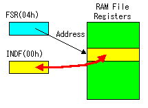
By this process, it shifts the message to be displaying to the left for one row and displays new messages in the row on the rightmost side. First, it shifts 2dn row messages to left. And 3rd row to 2dn row and reprepeats shifting 15 times in amount. Indirect addressing is used for this process. The content of the memory which corresponds to the address which was set to the FSR register is stored in the INDF register. If changing the contents of the INDF register in this condition, the contents of the RAM memory can be changed. ;************** New data write Process ****************
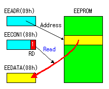
The read data is set to the row on the rightmost side of the LED display. By the above process, the display of the LED is shifted one row to the left. After reading the last data which was written in the EEPROM is done, it returns to the head data. By this processing is repeatedly done, the data of the EEPROM is displayed to flow on the LED screen. ;********************************************************
; END of signboard control processing
;********************************************************
end
|
||||||||||||||||||||||||||||||||||||||||||||||||||||||||||||||||||||||||||||||||||||||||||||||||||||||||||||||||