PIC16F84A Detailed specification (2)
|
In this page, I will explaine about the specification of the I/O ports of the PIC16F84A.
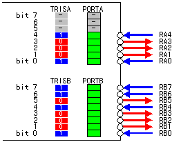
The A port and the B port rather differently in the circuit and the function. Also, in the A port, the RA4 pin can be used as the clock input of the TMR0. In case of the B port, from RB4 to RB7 have the function to watch over the change of the input signal. Moreover, RB0 has an external interrupt function. These functions confuse you. These functions are a convenient function but are not an indispensable function. Examine when those functions become necessary. Below, I will explain the outline of each port circuit. 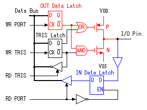 The figure on the left shows the circuit block of RA0, RA1, RA2 and RA3 at the A port. The data output circuit is composed of the output data latch register and CMOS drive circuit. The circuit of the CMOS has the function to block an output data to the pin of the input setting as well as the driving function in the output. The CMOS(Complementary-Metal Oxide Semiconductor) is the circuit which combined the N-channel MOSFET(N-FET) and the P-channel MOSFET(P-FET).
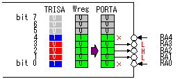
The mode of each pin is set with the TRISA register. The set value of the TRISA register is recorded to the TRIS latch register. The inverted output (
The input circuit is always connected with the I/O pin. So, even if it is set to the output mode, the input circuit is working. The input signal is taken into the input data latch register through the TTL buffer. The transfer of the input data to the output data latch register, the setting data to the TRIS latch register and the output data of the input data latch register is done through the data bus. The data bus has eight lines and the transfer of the data with the pins is done in parallel. Because the data bus is common use, the transfer of the information is controlled by the timing pulse of the control signal to each register. 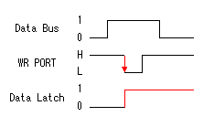 When wanting to output the contents of the PORTA register, first, the data of the PORTA register is set to the data bus. Next, the control signal of the output data latch register(WR PORT) is changed to the L level from the H level and the data of the bus is recorded to the data latch register. The contents of the output data latch register become the condition of the pin just as it is. After that, even if the data on the bus changes, the contents of the output latch register don't change until the control signal changes into the L level again from the H level. When wanting to output the contents of the PORTA register, first, the data of the PORTA register is set to the data bus. Next, the control signal of the output data latch register(WR PORT) is changed to the L level from the H level and the data of the bus is recorded to the data latch register. The contents of the output data latch register become the condition of the pin just as it is. After that, even if the data on the bus changes, the contents of the output latch register don't change until the control signal changes into the L level again from the H level.
The inverter with the gate is used for the reading of the contents of the TRIS latch register. The contents of the TRIS latch register are set on the data bus when RD TRIS becomes "1". 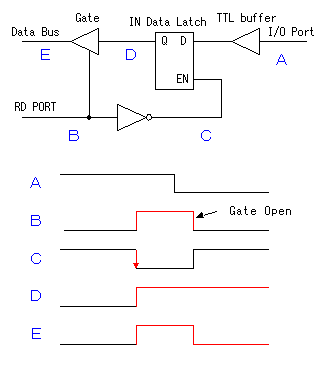 In the A port, RA4 is the port which has a special function. The figure below shows the circuit block of RA4. The difference with the other port is the FET for the output drive be only N-FET and the Schmitt trigger type is used as the input buffer. 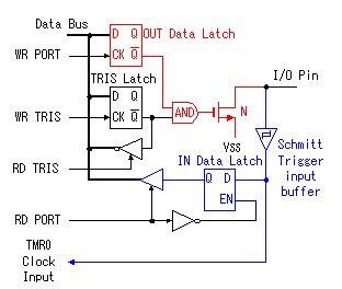 This pin can be used for the input of the clock timing pulse of TMR0 in case of the input mode. Because it is using the Schmitt-type input buffer, it can make the judgement of the H level or the L level, when the edge(rising or falling) of the external signal isn't clear. Because there is not P-FET of the output driver, the pull-up(It connects with VDD through the resistor) must put with the circuit outside to input H level. Because this circuit becomes an open drain type in the output mode, it is sometimes convenient for the design of the external circuit. 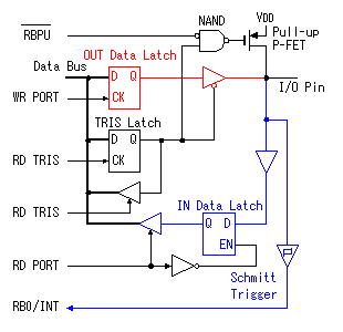 The output circuit composition of the B port is different from the A port. It doesn't use the FET for the output circuit and it is changing the mode with the gate circuit. The characteristic of the B port is to be equipped with the pull up function at the time of the input mode. The pull-up is to hang the input port on the side of the VDD. In this way, when the input is opening, the input port keeps H level. At usual circuit, the resistor is used for the pull-up but the FET is used at this circuit. The FET is not in the true ON condition and is made the weak pull-up condition. When this pull-up function influences circuit operation, it is possible to make not use. RB0 can be used as the input pin of the external interrupt, and is connected with the inner circuit through the Schmitt-type buffer. When the TRIS is "0", it is the output mode. Because there is an inverter in the control input of the output gate, the gate opens when the output of the TRIS latch register is "0" (the L level). The input of the NAND gate for the pull-up is the L level and the output is H level. Therefore, P-FET for the pull-up becomes OFF condition and pull-up isn't done. When the TRIS is "1", it is the input mode. The output gate is closed and output signal is separated from the I/O pin. As the side of the TRIS latch of the NAND gate for the pull-up is H level, pull-up or not is decided by the setting of the RBUP. RBPU is the bit 7 of the OPTION-REG register and is "Pull-up" in "0" and "Non pull-up" in "1". In case of "0", the gate of P-FET becomes L level and P-FET becomes ON condition. In case of "1", it is opposite. In RBPU, a whole B port pull up condition is set. It isn't possible to do setting every each pin. 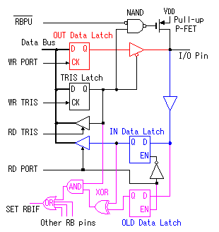 RB7 from RB4 has the function to detect the change of the input signal as well as the data input function. This function can be used the interruption processing by the key depression and so on. The change detection is done at the same time in four pins. Because it is, the change only of the specific pin can not be detected. This function works in case of the input mode in the pin. The OLD data latch register and the Exclusive OR(XOR) circuit are used for the change detection in addition to the input data latch register. RB7 from RB4 has the function to detect the change of the input signal as well as the data input function. This function can be used the interruption processing by the key depression and so on. The change detection is done at the same time in four pins. Because it is, the change only of the specific pin can not be detected. This function works in case of the input mode in the pin. The OLD data latch register and the Exclusive OR(XOR) circuit are used for the change detection in addition to the input data latch register.The input and the output of XOR are as follows. 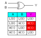 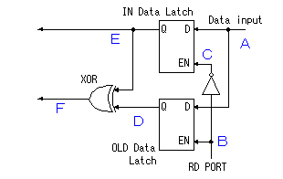 The operation of the input change detector is as follows. The input data is read to the input data latch register through the inverter when RD Port changes into the H level from the L level. At this time, reading to the OLD data latch registe isn't done yet. Next, the input data is read to the OLD data latch registe when RD Port changes into the L level from the H level. Because the output of each register is the same if there is not a change in the input, the output of XOR is L level. 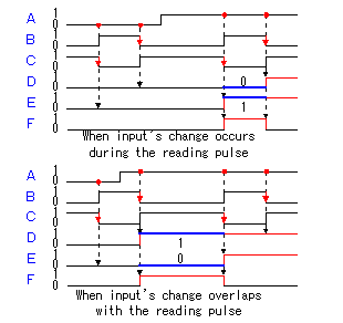 It supposes that the input data changed until the following reading timing. When RD Port becomes H level from the L level, the input data is read to the input data latch register. At this time, the contents of the OLD data latch registe aren't changing yet. Therefore, a different condition is inputted to the two inputs of XOR and H level is output. This H level becomes the trigger of the interruption signal. When RD Port becomes L level from the H level, the input data is read to the OLD data latch registe, the output of both registers becomes the same and the output of XOR becomes L level. When the input data is changed before the signal of RD Port becomes L level from the H level, the input data is read to the OLD data latch registe. On this point, because this change isn't read to the input data latch register yet, the condition of the output of both registers is different, H level is output by XOR and the interruption occurs. The output of XOR continues to the timing of the following RD Port reading pulse. I don't find an influence over the operation that this continues interruption. The interruption may occur once again when the output of XOR is H level even if it processes a interruption softly and it clears RBIF bit. Or, there is possibility to be guarded with the circuit inside. |
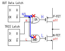
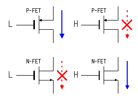 In case of the P-FET, when the gate becomes L level, it becomes ON condition and, when becoming H level, it becomes OFF condition. Oppositely, in case of the N-FET, when the gate becomes L level, it becomes OFF condition and, when becoming H level, it becomes ON condition. In case of being H level in the condition to want to output, the inverted output(
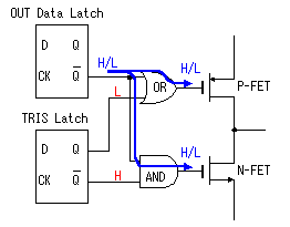 To set the output mode, it makes the bit of the TRISA register which corresponds to the pin "0". Because the output (Q) of the TRIS register is L level, the condition of the inverted output (