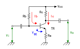
Basic circuit Basic circuit
The current feedback bias type amplifier is the amplifier which is putting the resistor between the emitter and the grounding. With the resistor of the emitter, it does the operation that the base electric current decreases by emitter voltage's going up when the collector electric current increases. It is called "the current feedback bias type amplifier" to control the base electric current of the input by the value of the emitter electric current.
Generally, at the electric current return-type amplifier, it attempts the alternating current signal gain improvement to connect the by-pass capacitor with the emitter resistor in parallel and it makes the influence of the circuit operation by the difference with the hFE value little to puts the resistor (the bleeder resistor:The resistor to continue to pass the electric current) between the base and the ground. The circuit this time omits them to make the parts little. This time, they don't influence mainly.
 The gain(G) The gain(G)
The gain is the ratio with the input signal voltage (Vi) and the output voltage (Vo).
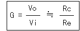
It is the ratio of the collector resistance (Rc) and the emitter resistance (Re) approximately.
Because phase of the input and the output shifts by the 180 degrees, it sometimes represents as G=-(Rc/Re), too. It is because the output voltage falls when input voltage goes up.
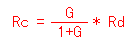
The calculation of each resistance value
It makes Rd=Rc+Re to make it easy to see the formula.
 The calculation of the collector resistance value The calculation of the collector resistance value
Rc=G*Re=G*(Rd-Rc)=G*Rd-G*Rc
Rc+G*Rc=G*Rd
Rc(1+G)=G*Rd
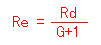
The calculation of the emitter resistance value
Re=Rc/G=(Rd-Re)/G
G*Re=Rd-Re
G*Re+Re=Rd
Re(G+1)=Rd
The calculation of the base resistance value
The electric current which flows through the emitter is total value of Ic and Ib. Ib is very small(1/hFE) compared with Ic. So, in above-mentioned calculation, it ignores.
Operation of the transistor amplifier
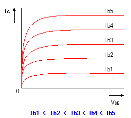
The figure on the left shows the characteristic of the transistor operation.
When the base electric current(Ib) is constant, even if the voltage between the collector and the emitter(VCE) changes, the collector electric current(Ic) doesn't change too much.
However, you find that the collector electric current changes when the base electric current changes.
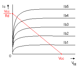
The red line of the figure on the left is the load line. When the base electric current is changed, the voltage between the collector and the emitter (VCE) and the collector electric current (Ic) change according to this line.
The maximum of the collector electric current(Ic) is when VCE is 0 V. It becomes the value which divided the power supply(Vcc) by total value(Rd) of the collector resistor(Rc) and the emitter resistor(Re). (It is in case of being ON in the fullness of the transistor(Saturation state))
The maximum voltage between the collector-the emitter(VCE) is the power supply(Vcc). (It is in case of being OFF in the fullness of the transistor)
The line which linked these points is the load line.
The load line of the figure is the load line in case of the direct current. Because the resistance value(Impedance) to the alternating current is related about the load line to the alternating current signal, the inclination is rather different.
The load line of the alternating current refer to the professional book.
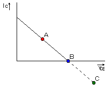
There are the class "A" amplification, the class "B" amplification, the class "C" amplification in the transistor amplifier according to the base electric current (the bias electric current) with the signalless condition.
The class "A" amplification is the amplifier which amplifies the signal of the same wave form as the input signal with usual amplifier. The bias operating point is the center of the load line. The voltage between the collector-the emitter(VCE) is about 1/2 of the power supply (Vcc).
The class "B" amplification is the way of being used for the push-pull amplifier. It is the way of amplifying the signal half. It combines the NPN-type transistor and the PNP-type transistor and the half is amplified. The output which is bigger than the class "A" amplification is gotten.
The class "C" amplification makes the bias point of the base electric current the side of the negative than the B point. It uses this way of being amplified for the amplification of the high frequency and so on. The distortion occurs to the output signal and can amplify the higher harmonic.
The operation of the class "A" amplification
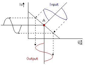
The signalless condition operating point of the class "A" amplification is in the center of the load line. So, both on the side of the positive of the input signal and the side of the negative voltage changes can be amplified.
In the small part of VCE, the base electric current and VCE aren't proportional. So, in case of the big input signal, the distortion occurs to the output.
In the figure, the output signal is smaller than the input signal and can be seen but the collector electric current is the mA and the base electric current of the input is the µA.
The operation of the class "B" amplification
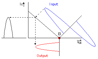
As for the class "B" amplification, it establishes the signalless condition operating point near the condition which the collector electric current(Ic) doesn't flow through. So, only the half of the input signal is amplified.
In the class "B" amplification, the two transistors combine and are used.
The characteristic of the direct current is opposite about the NPN and the PNP transistor. The half of the input signal can be amplified when combining these.
The operation of the class "C" amplification
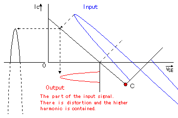
The operating point of the class "C" amplification is not on the load line.
The part of the input signal is amplified.
So, it isn't possible to use for the amplification such as the sound.
It is used for the high frequency multiplying circuit and so on.
|
Design for the transistor amplifier
I will show the result which calculated the value of each resistor of the amplifier which was used this time below.
hFE(DC current gain) of the transistor which was used this time was to do 115 being(Measurement value).
Generally, hFE of this transistor is about 180. Because I did the gain of the amplifier by 20 times this time, I chose the small one of hFE. The resistance value to put in the base becomes big when hFE is big.
The design condition
The power supply(Vcc) = 12V
The collector electric current(Ic) = 1mA
The gain (G) = 20
hFE = 115
The calculation of Rd
| Rd | = (Vcc/Ic)*(1/2) [To make the operating point the center of the load line] |
| = 12V/(1mA*2) |
| = 6K-ohm |
The calculation of Re
| Re | = Rd/(G+1)=Rd/21 |
| = (6 x 10³ohm)/21 |
| = 286-ohm [220-ohm is used at the actual circuit] |
The calculation of Rc
| Rc | = (Rd*G)/(1+G))=20Rd/21 |
| = (20 x 6 x 103ohm)/21 |
| = 5714-ohm [5.6K-ohm is used at the actual circuit] |
The resistance value which was used with the actual circuit is different from the calculation value. However, there is no problem.
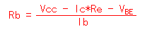
The calculation of Rb
| Rb | = (Vcc-(Ic*Re)-VBE)/(Ic/hFE) |
| = (12V-(1mA x 220ohm)-0.7V)/(1mA/115) |
| = (12-0.22-0.7) x 115 x 103 |
| = 1,274 x 103 |
| =1.274M-ohm [1M-ohm and 220K-ohm are used at the actual circuit] |
Actually, the voltage between the collector and the grounding when using above-mentioned resistance value was to 6.15 V be.
|