The operation explanation
of MC34063A
|
I explain that the circuit works based on the block diagram of MC34063A in this page. The block diagram refer to "Switching regulator (2)". The MC34063A is composed of the following functional block. Hereinafter, I explain that each block works. The explanation goes by the understanding of me based on the block diagram. So the details may be different.  The reference voltage comparison block The reference voltage comparison blockThe reference voltage is 1.25 V. It detects whether or not the comparative voltage to have made with the output voltage is lower or higher than the reference voltage with the comparator. The switching regulator injects the electric power to the output from the input if the comparative voltage is lower than the reference voltage and works to restrain the electric power to the output if the comparative voltage is high. The side of the negative of the reference voltage may are not the grounding. With this, the regulator can work in the inverting. 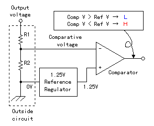 The comparative voltage is made by the voltage drop of R1 and R2. R1 and R2 are the external part. The comparative voltage is connected with the negative input of the comparator. The 1.25-V voltage is output from the reference regulator. The reference voltage is connected with the positive input of the comparator. When the comparative voltage is higher than the reference voltage, the output of the comparator becomes the L level. When the comparative voltage is lower than the reference voltage, the output of the comparator becomes the H level. I explain behind, the regulator restrains the supply of electric power to the output when the output of the comparator becomes the L level. The supply of electric power is worked when the output of the comparator becomes the H level. You can change the output voltage by changing the value of R1. In case of the step-up or the step-down converter, the external circuit makes be introducing in this corner. 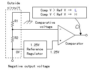 In case of the inverting converter, you make the external circuit like the figure on the left. The electric current which flows through R2 increases when the output voltage becomes high on the side of the negative. With it, the voltage of the both edges of R2 goes up. Then, the comparative voltage becomes higher than the reference voltage and the output of the comparator becomes the L level. The supply of electric power to the output is restrained by it and the output voltage becomes low to the side of the positive. When the output voltage becomes low on the side of the positive, voltage of R2 goes down and the comparative voltage becomes lower than the reference voltage. In the case, the output of the comparator becomes the H level, the supply of electric power to the output is done and the output voltage becomes high to the side of the negative. You can change the output voltage by changing the value of R1. The oscillation circuit block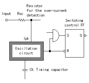 The oscillation frequency (the switching frequency) can be changed with the capacitor of the external. The output of the oscillation circuit is applied to the flip-flop for the switching control and drives the switching transistors. The oscillation circuit manages the function of the over-current detection more. It detects the voltage of the over-current detection resistor which is inserted in the input circuit. In case of the over-current condition, it restrains the oscillation operation and it protects the switching transistors from the destruction. The detection voltage of the over-current is 0.3 V. This time, I used the 0.22-ohm resistor as Rsc. The upper limit value of the input electric current becomes 0.3V / 0.22ohm = 1.36 A. Because the consumption electric power of the resistor was (1.36A)2 x 0.22ohm = 0.41 W, I used the 1-W one. The figure below is the graph which shows the relation between the timing capacitor and the oscillation frequency which is in the data sheet. 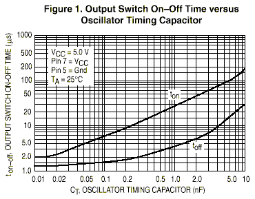 With this chart, you find the thing with the longer time that the switch is ON as the output of the oscillator. When using the 470-pF capacitor, it becomes ton = 20µS, toff = 3µS. The frequency is 1 / (20 x 10-6 + 3 x 10⁻⁶) = 43kHz. At 100 pF, it becomes 1/(7x10-6+1.5x10-6) = 118kHz. As for this chart, Vcc is in case of 5 V. Because it is, it becomes the value which depends a little on the input voltage to use. When high-frequency, the coil to use with the ripple filter circuit can be made small. However, the loss with the fly-wheel diode(I use the Shottky barrier diode) becomes big. I think that you had better use at less than 100-kHz frequency. The switching block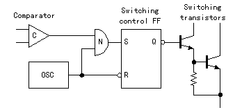 The switching transistors are controlled by the output of the comparator and the output of the oscillator. The SR-type flip-flop (FF) is used for the control of the transistor. The Q becomes the H level when S becomes the L level in SR-FF. However, as for the FF which is used here, the inverter (making the L and H opposite) is added to the output. In the explanation of the following of me, it makes the output of the inverter the Q. The Q becomes the L level when S becomes the L level. Also, the Q becomes the H level when R becomes the L level. When S is the L level, irrespective of the condition of R, the Q becomes the L level. This inverter isn't written at the data sheet. The inverter is necessary when thinking of the regulator operation. The white circle expresses the inverter by the circuit diagram. Because the switching transistor becomes OFF when the comparative voltage is higher than the reference voltage when confirming in the operation by the actual IC, you find that the inverter is added.
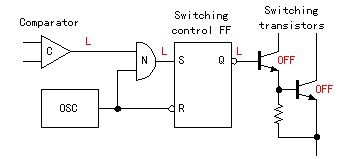 When the comparative voltage is higher than the reference voltage, the output of the comparator (C) becomes the L level. When any one of the input of the NAND gate (N) becomes the L level, the output becomes the L level. Because it is, in this case, irrespective of the output of the oscillator (OSC), S becomes the L level. When S is the L level, the Q, too, becomes the L level and the switching transistors become the OFF condition. When the switching transistors are OFF, the supply of electric power to the output is restrained and the output voltage falls.
 When the comparative voltage is higher than the reference voltage, the output of the comparator (C) becomes the H level. In this case, the output of the NAND gate (N) changes according to the condition of the oscillator (OSC). When the output of the OSC is the H level, the output of N becomes H. The inverter is added to R, too. Because it is, when the output of the OSC is H, R becomes the L level and the becoming Q becomes the H level. When the Q becomes H, the switching transistors become the ON condition. 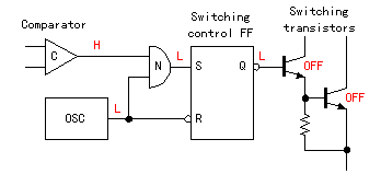 When the output of the OSC is the L level, the output of N, too, becomes the L. In this case, because the Q becomes the L, the switching transistors become the OFF condition.
|
||||||||||||