[Menu]>[Electronic circuit beans collection]>[PLL synthesizing oscillator (1)]>[Circuit explanation]

PLL frequency synthesizer
(MB87014A)


Block diagram of the top is a clickable image map.
You can jump to each page of the explanation when you click each block.


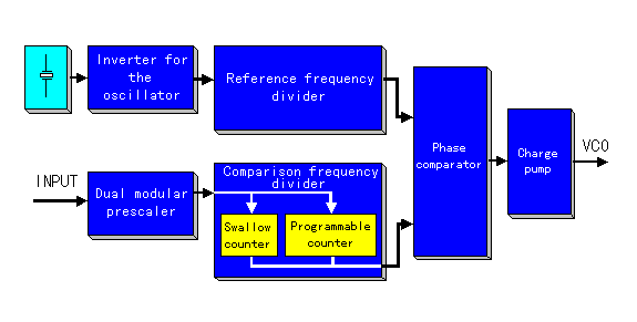
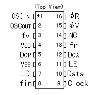
MB87014A is the IC for the PLL synthesizer which was made with CMOS.
The shape is SMT(Surface Mount Type) in DIP(Dual In Line Package) of 16pins.
This IC is composed of the following functional block.

The inverter for the oscillatorThe reference frequency (being 2 MHz this time) circuit for the crystal oscillator
The reference frequency dividerThe circuit which divides a reference frequency to the phase comparison frequency
Dual modular prescalerThe circuit which divides a comparison frequency in 64
The comparison frequency dividerThe circuit which divides the frequency of the outside VCO to the phase comparison frequency
The phase comparatorThe circuit which compares a phase comparison frequency
The charge pumpThe circuit which outputs the result which compared a phase to the outside lowpass filter

The operation possible frequency is to 180 MHz in the specification.

The singular point of this IC is to use serial data to specify the dividing ratio of the reference frequency divider and the comparison frequency divider.
This singular point is good because it can rarely do the IC number of pin but the serial data generation circuit which specifies a dividing ratio becomes necessary.
It may be that there is dividing ratio setting IC or a circuit for this IC. Because the PLL to introduce this time is the purpose to output the frequency of the fixation, it is made to make serial data with the initialization circuit as the initial setting operation in case of the turning on.
Because it composed in the general logic ICs, it became a comparatively big circuit. At the actual printed board, most are the space of this initialization circuit.


Input/output signal and the function

Term
No.
Term
name
I/OFunction explanation
1OSCINI The connection terminal of the crystal oscillator and the capaitors
It is possible to input a clock from outside, too, from OSCIN.
2OSCOUTO
3fvOThe output terminal of the comparison frequency divider
4VDD-The power supply terminal
5DOPOThe lowpass filter connection terminal (For the passive)
6VSS-The grounding terminal
7LDO The output terminal of the phase comparator
When locking, it outputs "H" and when the lock comes, it outputs " negative pulse ".
8finI The comparison frequency input terminal
(It makes an AC connection).
9ClockI The clock input terminal of the data which sets a dividing ratio
It reads data in the rise of the clock pulse.
10DataIThe input terminal of the data which sets a dividing ratio
11LEI The load enable input terminal
It sends the contents of Data to the side of the reference or the side of the comparison in the combination with the control bit of Data at the time of LE=H.
12DOAOThe connection terminal of the lowpass filter (For the activist)
13frOThe output terminal of the reference frequency divider
14NC-The non connected terminal
15VOThe lowpass filter connection terminal (For the differential-type filter)
16RO


Crystal oscillator


It is the one to have installed a pole in the crystal to have made shaped like the board thin. The frequency is decided by the thickness of the crystal board.
It is possible to make oscillate a specific frequency by the stability.


Dividing ratio of the programmable divider
    The Data form
      Data(10th pin) to set the dividing ratio of the programmable divider needs the following form.


    The specification range with dividing ratio

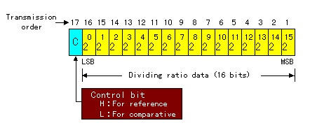
      It specifies a dividing ratio by 16 bits as mentioned above both for the reference frequency divider and the comparison frequency divider.
      However, the handling differs in the reference frequency divider and the comparison frequency divider.

      In case of the reference frequency divider

        It handles 16 bits as one data block.
        The specification range is possible to 5 - 65535.

      In case of the comparison frequency divider

        It handles 16-bit data, dividing it into two blocks. It is 20-25, and 26-215.
        It handles 20-25 6 bits with the swallow counter and it handles 26-215 with the programmable counter. It is a specification range below each.
        The swallow counter: 0 - 63
        The programmable counter: 5 - 1023

        Because it is, the range where the comparative divider can be specified becomes by 320 - 65535.
          Swallow
          Programmable
          specification value
          0
          5(x64)
          320
          1
          5
          321
          2
          5
          322
          :
          :
          :
          63
          5
          383
          0
          6
          384
          :
          :
          :
          62
          1023
          65534
          63
          1023
          65535


    The timing of the data and the control signal


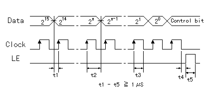
      Data is read at the time of the rise of Clock.
      When the LE is H level, Data part is read by the appropriate counter. When the control bit in the Data part is H, it becomes data for the reference frequency divider and in case of the L, it becomes data for the comparison frequency divider.


    The standby mode
      When data (16 bits) which sets a dividing ratio is all zero (the L level), the operation of the PLL circuit stops and each input level of fin, OSCIN becomes H level compulsorily.(Low consumption electric power)
      This condition is canceled when specifying data except "all zero".


Inverter for the oscillator
    It is the inverter circuit to make oscillate a crystal oscillator.
    The output of the inverter is returned to the input of the inverter through the crystal oscillator. By this, it makes do the oscillation which was stable at the natural frequency of the crystal oscillator.


Dual modular prescaler
    It is using the dual modular prescaler to divide in 64 for the dividing of a comparison frequency.
    10 bits of higher ranks of the dividing ratio setting data (16 bits) are used as the set value of the programmable counter.


Phase comparator
    It detects the difference of the phase comparison frequency which was divided with the reference frequency divider and the comparison frequency divider.
    The relation of the output of each input frequency and phase comparator and charge pump becomes like the following figure.

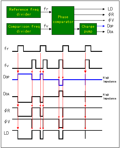
There are five kinds pieces of output.

The circuit this time is using DOP output for the passive lowpass filter.
As for this output, when fv is low (the period is long), the positive signal which accepted a fimite difference is output by DOP.
It is using a varicap diode for the frequency adjustment by VCO to be explaining in the circuit explanation of the VCO. The capacitance of the diode becomes small when the voltage becomes high.
Because it is, the capacity of the varicap becomes small when the voltage which is output from DOP becomes positive and the oscillation frequency of the VCO becomes high.

When fv is high (the period is short), the negative signal which accepted a fimite difference is output by DOP.
The voltage which is gained by the varicap by this becomes low and the capacity of the varicap becomes big. Because it is, the oscillation frequency of the VCO becomes low.

The control of the oscillation frequency of the VCO is done in this way.

    Because the circuit this time is using a varicap, it is necessary to make the condition to have always added positive voltage.
    Because it is, it works in the condition of fr > fv.


Charge pump
    It has two kinds of charge pumps(For the activist and for the passive).
    It outputs below by the relation in reference frequency (fr) and comparison frequency (fv).
For the activistfr > fvSink mode (Output DOA=L level)
fr = fvHigh impedance condition
fr < fvDrive mode (Output DOA=H level)
For the passivefr > fvDrive mode (Output DOP=H level)
fr = fvHigh impedance condition
fr < fvSink mode (Output DOP=L level)


    MB87014A can use an outside charge pump, too.
    The result of the phase comparator is directly output by LD terminal (7th pin).
    The output contents are as follows.
For the differential-type filterfr > fvV = H , R = L
fr = fvV = H , R = H
fr < fvV = L , R = H


Rating
    The maximun rating

ItemSymbolRated valueUnit
Power supply voltageVDDVSS-0.3 to VSS+6.0V
Input voltageVINVSS-0.3 to VDD-3.0V
Output voltageVOUTVSS-0.3 to VDD-3.0V
Output currentIOUT±10mA
Operating temperatureTa-30 to 80°C
Power consumptionPD300mW


    The recommendation operation condition

ItemSymbolStandard valueUnit
Power supply voltageVDD4.5 to 5.5(VSS = 0V)V
Input voltageVINVSS to VDDV
Operating temperatureTa-30 to 60°C