Microelectronics I Notes Supplement
Latchup in Bulk CMOS
A byproduct of the Bulk CMOS structure is a pair of parasitic bipolar
transistors. The collector of each BJT is connected to the base of the other
transistor in a positive feedback structure. A phenomenon called latchup
can occur when (1) both BJT's conduct, creating a low resistance path between
Vdd and GND and (2) the product of the gains of the two transistors
in the feedback loop, b1 x b2, is greater than one. The result of latchup
is at the minimum a circuit malfunction, and in the worst case, the destruction
of the device.
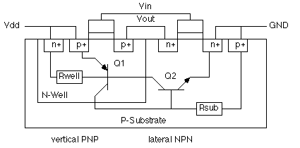
Cross section of parasitic transistors in Bulk CMOS
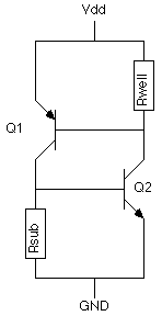
Equivalent Circuit
Latchup may begin when Vout drops below GND due to a noise spike or an improper
circuit hookup (Vout is the base of the lateral NPN Q2). If sufficient current
flows through Rsub to turn on Q2 (I Rsub > 0.7 V ), this will draw current
through Rwell. If the voltage drop across Rwell is high enough, Q1 will also
turn on, and a self-sustaining low resistance path between the power rails
is formed. If the gains are such that b1 x b2 > 1, latchup may occur.
Once latchup has begun, the only way to stop it is to reduce the current
below a critical level, usually by removing power from the circuit.
The most likely place for latchup to occur is in pad drivers, where large
voltage transients and large currents are present.
Preventing latchup
Fab/Design Approaches
-
Reduce the gain product b1 x b1
-
move n-well and n+ source/drain farther apart increases width of the base
of Q2 and reduces gain beta2 > also reduces circuit density
-
buried n+ layer in well reduces gain of Q1
-
Reduce the well and substrate resistances, producing lower voltage drops
-
higher substrate doping level reduces Rsub
-
reduce Rwell by making low resistance contact to GND
-
guard rings around p- and/or n-well, with frequent contacts to the rings,
reduces the parasitic resistances.
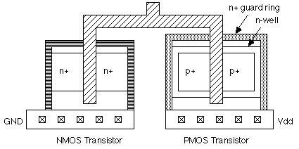
CMOS transistors with guard rings
Systems Approaches
-
Make sure power supplies are off before plugging a board. A "hot plug in"
of an unpowered circuit board or module may cause signal pins to see surge
voltages greater than 0.7 V higher than Vdd, which rises more slowly to is
peak value. When the chip comes up to full power, sections of it could be
latched.
-
Carefully protect electrostatic protection devices associated with I/O pads
with guard rings. Electrostatic discharge can trigger latchup. ESD enters
the circuit through an I/O pad, where it is clamped to one of the rails by
the ESD protection circuit. Devices in the protection circuit can inject
minority carriers in the substrate or well, potentially triggering latchup.
-
Radiation, including x-rays, cosmic, or alpha rays, can generate electron-hole
pairs as they penetrate the chip. These carriers can contribute to well or
substrate currents.
-
Sudden transients on the power or ground bus, which may occur if large numbers
of transistors switch simultaneously, can drive the circuit into latchup.
Whether this is possible should be checked through simulation.